The figure below is a step-down switching power supply that converts a 12V input voltage into a 3.3V output voltage with an output current of up to 3A. An integrated power controller (Semtech model SC4519) is used on this power supply. This controller integrates a power tube into the power controller chip. This kind of power supply is very simple, especially suitable for consumer electronics such as portable DVD players, ADSL, set-top boxes.
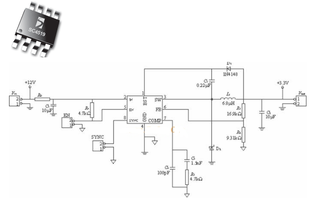
Figure SC4519 consists of 12V to 3.3V, 3A switching power supply circuit
As with the previous example, for this simple switching power supply, the following points should also be noted when designing the PCB.
1) The loop area enclosed by the input filter capacitor (C3), SC4519 grounding pin (GND), and D2 must be small. This means that C3 and D2 must be very close to the SC4519.
2) A separate power circuit ground plane and control circuit ground plane can be used. Components connected to the power ground include input socket (VIN), output socket (VOUT), input filter capacitor (C3), output filter capacitor (C2), D2, SC4519. Components connected to the control ground include output divider resistors (R1, R2), feedback compensation circuits (R3, C4, C5), enable socket (EN), and synchronous socket (SYNC).
3) Add a via hole near the grounding pin of SC4519 to connect the power circuit ground plane to the grounding layer of the control signal circuit.
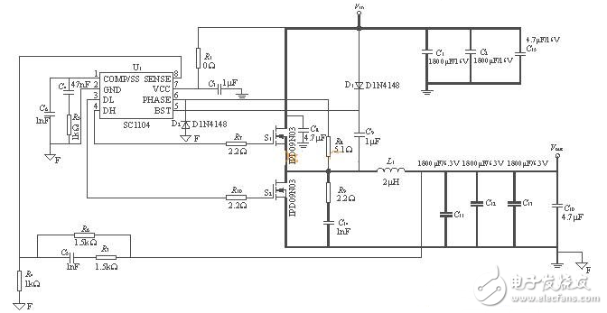
12v to 3.3v circuit diagram (2)The following figure is a schematic diagram of a buck switching power supply applied to consumer electronics. The designer should be able to distinguish the components in the power circuit and the components in the control signal circuit on this circuit diagram. If the designer treats all the components in the power supply as components in a digital circuit, the problem can be quite serious. It is usually first necessary to know the path of the high frequency current of the power supply and to distinguish between small signal control circuits and power circuit components and their routing. Generally speaking, the power circuit of the power supply mainly includes an input filter capacitor, an output filter capacitor, a filter inductor, and an upper and lower power FET. The control circuit mainly includes a PWM control chip, a bypass capacitor, a bootstrap circuit, a feedback voltage dividing resistor, and a feedback compensation circuit.
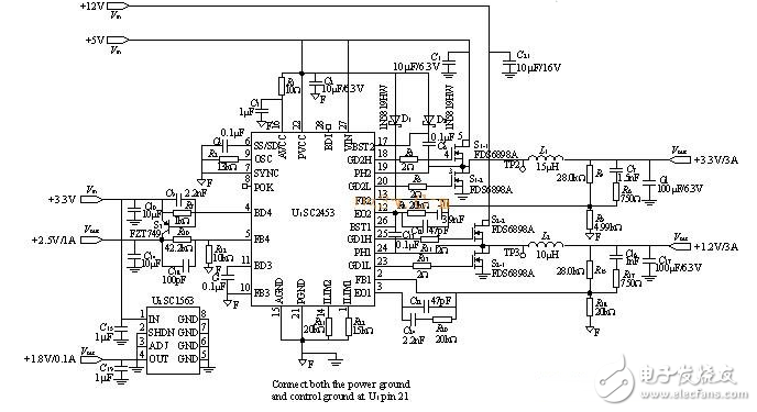
This power supply has three sets of input voltages (12V, 5V and 3.3V) and four sets of output voltages (3.3V, 2.6V, 1.8V, 1.2V). The power supply uses an integrated multiplexer controller (Semtech model SC2453). The SC2453 offers a wide input voltage range of 4.5V to 30V, two switching frequency up to 700kHz and up to 15A output current, and a synchronous buck converter with output voltage as low as 0.5V. It also offers a dedicated adjustable positive pressure linear regulator and a dedicated adjustable negative pressure linear regulator. The TSSOP-28 package reduces the required board area. Two out-of-phase buck converters reduce input current ripple. The figure below is a schematic diagram of this multi-way switching power supply. The 3.3V output is generated by a 5V input, the 1.2V output is generated by a 12V input, and the 2.6V and 1.8V outputs are generated by a 3.3V input.
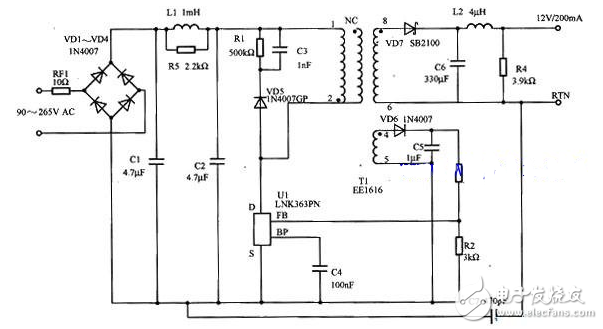
The figure shows the 2.4W/12V output switching power supply circuit. The circuit is a low cost, small component count, small and lightweight, and can replace the linear power supply solution. The circuit does not require an optocoupler and is extremely energy efficient, meeting the CEC requirements for efficiency in the load mode (required 57.9%, up to 66%), and low power consumption at no load (less than 300mW at 265VAC AC input), Compliant with the EMI limit requirements of ClSPR-22/EN55022B, the EMI margin is greater than 8dBuV. It can convert the AC input voltage in the range of 90 ~ 265VAC into a single isolated DC voltage output, the power output is 12V / 200mA (2.4W), and has constant IV constant current (CV / CC) characteristics.
The circuit of Figure 1 boosts the -12V voltage to 15.3V (relative to -12V), resulting in a 3.3V supply voltage with an output current of 300mA. Q2 converts the 3.3V voltage into an appropriate voltage (-10.75V) and feeds it back to the FB pin of IC1. The PWM boost controller can provide 1W of output power with a conversion efficiency of 83%. The whole circuit occupies a circuit board size of 6.25cm2, which is suitable for applications that rely on desktop PC power supply and needs to provide 1W output power. In this application, since the -12V bus voltage is limited to 1.2W, it needs to be higher than 83% conversion efficiency.
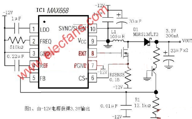
Universal multi-supply buses, such as VME, VXI, and PCI buses, provide power-limited 3.3V, 5V, and ±12V (or ±24V) power supplies. If devices (such as cards) are added to these systems, An additional 3.3V or 5V supply, which is typically supplied by a lightly loaded -12V supply. The circuit uses the MAX668 chip. Since the current limiting resistor (RSENSE) limits the peak current to 120mA, the N-channel MOSFET (Q1) can be selected with an inexpensive logic-level driven FET, and R1 and R2 set the output voltage (3.3V or 5V). The feedback voltage of the IC1 balanced terminal (Pin5) is higher than the PGND pin (Pin7) 1.25V, so:
VFB=-12V+1.25V=-10.75V
After selecting resistor R1, you can determine:
I2=1.25V/R1=1.25V/12.1kΩ=103μA
R2 can be determined by:
R2=(VOUT-VBE)/I2=(3.3V-0.7V)/103μA=25.2kΩ
In Figure 1, the switching frequency of IC1 is allowed to be set by an external resistor. The frequency range is from 100kHz to 500kHz, which is beneficial to the design of RF, data acquisition modules and other products. When a higher switching frequency is selected, higher conversion efficiency can be ensured, and smaller inductors and capacitors can be selected. To avoid current backflow, add a diode in series with R1 in the circuit.
Laptop Stand Macbook Air,Laptop Stand Macbook Air Black,Laptop Stand Macbook Pro Vertical,Laptop Stand Macbook Travel,etc.
Shenzhen Chengrong Technology Co.ltd is a high-quality enterprise specializing in metal stamping and CNC production for 12 years. The company mainly aims at the R&D, production and sales of Notebook Laptop Stands and Mobile Phone Stands. From the mold design and processing to machining and product surface oxidation, spraying treatment etc ,integration can fully meet the various processing needs of customers. Have a complete and scientific quality management system, strength and product quality are recognized and trusted by the industry, to meet changing economic and social needs .

Laptop Stand Macbook Air,Laptop Stand Macbook Air Black,Laptop Stand Macbook Pro Vertical,Laptop Stand Macbook Travel
Shenzhen ChengRong Technology Co.,Ltd. , https://www.laptopstandsupplier.com