Dual port RAM is widely used in heterogeneous systems. Through dual-port RAM, chips with different hardware architectures can realize data interaction and realize communication. For example, in general, the communication between ARM and DSP can be realized by dual-port RAM. The ARM is connected to the A port of the dual-port RAM through the EBI bus. The DSP passes the EMIF bus (it can also be the uPP bus, depending on the speed requirement). Connected to the B port of the dual-port RAM, the two operate on the same storage area, and the data interaction between the two can be realized.
However, since the A and B ports of the dual port RAM can operate on the same memory address, this raises a problem - if the two parties simultaneously read and write to the same address on both ports, a conflict will be caused. There are two ways to solve this problem. First, the communication parties ensure that the same address is not read and written at the same time, and the ARM and DSP writable address ranges are partitioned. Whenever one of the parties finishes writing the data, the other party sends an interrupt to notify the other party, and the other party performs data reading (ping-pong RAM). Operation), this is more reliable; another way is to set the write busy signal in fpga to achieve write synchronization at both ends []. In FPGA, there are two ways to build dual-port RAM, one is to use distributed RAM and the other is to use Block RAM. For the specific difference between the two, you can refer to these two articles [][]. In short, the block RAM uses the entire block of dual-port RAM resources in the FPGA, while the distributed RAM is pieced together with the logical resources in the FPGA. The general principle is that for larger storage applications, it is recommended to use bram; sporadic small ram, generally use dram.
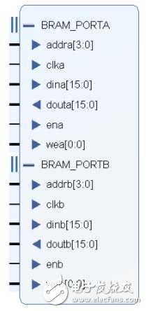
In Vivado, the RAM IP core is in the Memories & Strorage Elements\RAM & ROMs and RAM & ROMs & BRAM folders. As shown in the figure below, the Vivado dual-port RAM IP core is briefly introduced below.
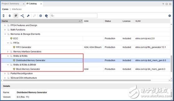
(Figure 1.1)
2.Vivado dual port RAM IP core2.1 Block Memory Generator Overview
Click on the Block Memory Generator item in Figure 1.1 to build a dual-port RAM using BRAM. The Block Memory Generator window is shown in Figure 2.1.
In the figure, in the first part, on the IP symbol tab, click the “+†sign to expand the port specific signal, as shown in Figure 2.2. In Part 2, Component Name can set the name of the IP core. Part 3, Basic tab, in the Memory Type drop-down list, you can set the type of memory, as shown in Figure 2.3. Block Memory Gnerator can generate 5 different types of memory space, including block RAM: single-port RAM, simplified dual-port RAM and true dual-port RAM []. The single-port RAM has only one port (A port), which can read and write to the A port. Simplified dual-port RAM has two ports (A and B ports), but the A port can only perform write operations and cannot perform read operations, while the B port can only perform read operations and cannot perform write operations. True dual-port RAM has two ports (A and B ports), and both A and B ports can be read and written [].
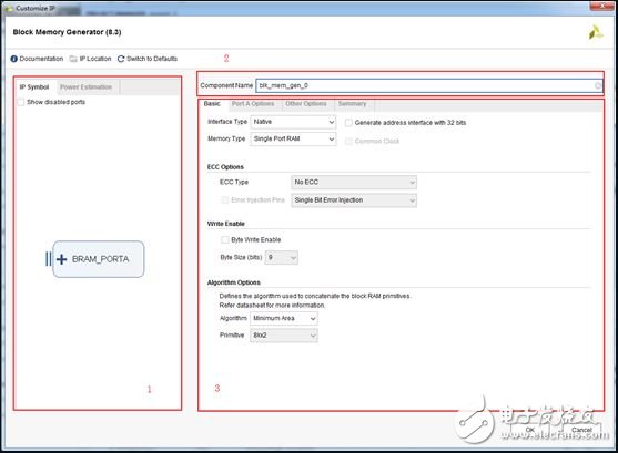
(Figure 2.1)
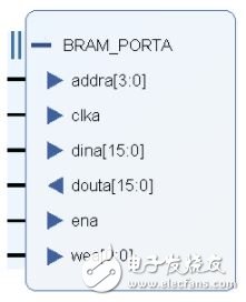
(Figure 2.2)
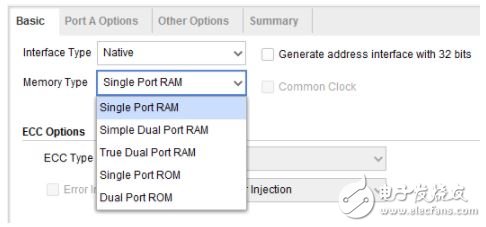
(Figure 2.3)
2.2 True Dual Port RAM Settings
2.2.1 Basic settings
Select True Dual Port RAM in the Memory type option of the Basic tab. The IP Symbol is shown in Figure 2.4. ECC OpTIons is the default setting. The default setting is also selected in Write Enable. Byte write is not enabled. Algorithm OpTIons selects the default setting.
(Figure 2.4)
2.2.2 Port Settings
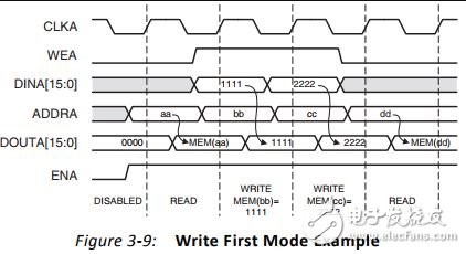
Click the Port A OpTIons tab to set the A port, set the Write Width to 16 (that is, the RAM unit is 16 bits), and the Write Width to 1024 (that is, the memory depth is 1024, the port can read and write RAM units have 1024) There are three types of OperaTIng Mode: Write First, Read First, No Change. In Write First mode, data written to the memory unit is synchronously output to the output data bus in one clock cycle; in Read First mode, the data written to the memory unit is the current input data in one clock cycle. The data on the bus, and the data output to the output data bus is the data stored in the memory unit in the previous clock cycle. For details, refer to pages 49 to 50 of PG058. Enable Port Type is set to Always Enabled, and port A is always enabled. Other settings use the default settings. As shown in Figure 2.5.
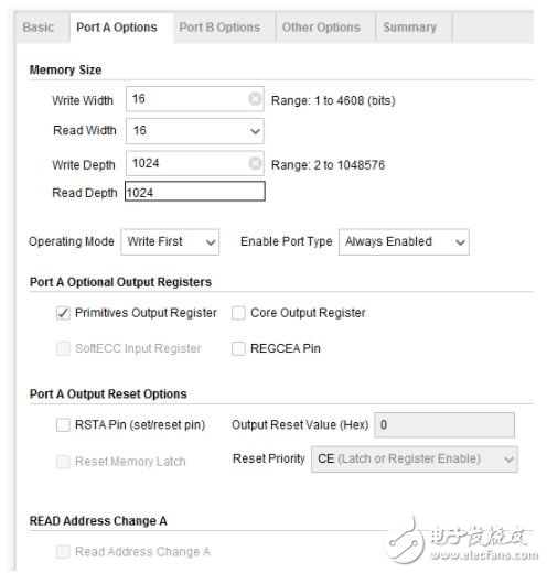
(Figure 2.5)
Port B is set to match A. In the Other Options tab, keep the default settings. Load Init File sets whether to initialize the memory area with the Coe file. This will be used when initializing the ROM. It is not checked here and remains the default. Finally, the consumed resources are displayed on the Summary tab.
3. Dual port RAM routineRoutine 1, this routine is Altera's official routine [], using registers to build dual-port RAM, the code is as follows:
Moduletrue_dpram_sclk
(
Input [7:0] data_a, data_b,
Input [5:0] addr_a, addr_b,
Input we_a, we_b, clk,
Outputreg [7:0] q_a, q_b
);
// Declare the RAM variable
Reg [7:0] ram[63:0];
// Port A
Always @ (posedge clk)
Begin
If (we_a)
Begin
Ram[addr_a] <<= data_a;
Q_a <<= data_a;
End
Else
Begin
Q_a <<= ram[addr_a];
End
End
// Port B
Always @ (posedge clk)
Begin
If (we_b)
Begin
Ram[addr_b] <<= data_b;
Q_b <<= data_b;
End
Else
Begin
Q_b <<= ram[addr_b];
End
End
Endmodule
Routine 2, this routine is the Xilinx official routine [], using registers to build a true dual-port RAM, the code is as follows:
// Dual-Port Block RAM with Two Write Ports
// File: rams_16.v
Modulev_rams_16 (clka,clkb,ena,enb,wea,web,addra,addrb,dia,dib,doa,dob);
Input clka,clkb,ena,enb,wea,web;
Input [9:0] addra, addrb;
Input [15:0] dia,dib;
Output [15:0] doa,dob;
Reg[15:0] ram [1023:0];
Reg[15:0] doa,dob;
Always @(posedge clka) beginif (ena)
Begin
If (wea)
Ram[addra] <<= dia;
Doa "= ram[addra];
End
End
Always @(posedge clkb) beginif (enb)
Begin
If (web)
Ram[addrb] <<= dib;
Dob "= ram[addrb];
End
End
Endmodule
Routine 3, this routine is a routine [] in the netizen blog, the code is as follows:
moduleTOP(
Input USER_CLK
);
`define DLY #1
Reg FPGA_Enable=0;
Reg[3:0] FPGA_Write_Enable=4'h0;
Reg[31:0] FPGA_Address=0;
Reg[31:0] FPGA_Write_Data=0;
Reg[31:0] FPGA_Read_Data_reg=0;
Wire[31:0] FPGA_Read_Data;
Reg[10:0] count=0;
Always @ (posedge USER_CLK)
Begin
Count "= count +1;
If(count"=100)
Begin
FPGA_Enable <<=0;
FPGA_Write_Enable <<=4'h0;
End
Elseif((count <<=105)&&(count 》100))
Begin
FPGA_Enable <<=1;
FPGA_Write_Enable <<=4'hf;
FPGA_Address <<= FPGA_Address +4;
FPGA_Write_Data <<= FPGA_Write_Data +1;
End
Elseif((count =110)&&(count 》105))
Begin
FPGA_Enable <<=0;
FPGA_Write_Enable <<=4'h0;
FPGA_Address <<=0;
FPGA_Write_Data <<=0;
End
Elseif((count <<=117)&&(count 》110))
Begin
FPGA_Enable <<=1;
FPGA_Write_Enable <<=4'h0;
FPGA_Read_Data_reg <<= FPGA_Read_Data;
FPGA_Address <<= FPGA_Address +4;
End
Elseif(count ==118)
Begin
FPGA_Enable <<=0;
Count "= count;
End
End
BBBByour_instance_name (
.clka(USER_CLK), // input clka
.ena(FPGA_Enable), // input ena
.wea(FPGA_Write_Enable), // input [3 : 0] wea
.addra(FPGA_Address), // input [31 : 0] addra
.dina(FPGA_Write_Data), // input [31 : 0] dina
.douta(FPGA_Read_Data), // output [31 : 0] douta
.clkb(clkb), // input clkb
.enb(enb), // input enb
.web(web), // input [3 : 0] web
.addrb(addrb), // input [31 : 0] addrb
.dinb(dinb), // input [31 : 0] dinb
.doutb(doutb) // output [31 : 0] doutb
);
Endmodule
In this routine, after the count is 101 ("100), writing to 1-5 is performed to addresses 4 to 20, and then the written data is read when count is 111 ("110).
4. SimulationLet's use Modelsim and Vivado for co-simulation. For how vivado can co-simulate with modelsim, you can refer to this article:
The connection between vivado and modelsim and device library compilation
One thing to note is that I am using Vivado 2017.1 version. This version only supports Modelsim10.5 and above. If it is a low version of Modelsim, it will make an error when compiling Modelsim's simulation library with Vivado2017.1. Modelsim version 10.5 can be downloaded here:
Modelim 10.5 for vivado 2017.1
When simulating with Modelsim, three .do files are generated in the sim_1/behav folder, which are xx_compile.do, xx_simulate.do, xx _wave.do files. After the design of the verilog file is modified, if you restart directly in Modelsim, the simulation still has no files before modification. To make the modified .v file take effect in Modelsim, you can enter the do xx_compile.do file in the Modelsim command window. Recompile the simulated library file and the design file (.v file), and then enter the do xx_simulate.do file to simulate the modified file. When you type the do xx_compile.do command to recompile the design file, Modelsim will force the exit, which is caused by the last sentence force quit command, just delete it. If you want to save the waveform file, you can save the format and save it as a xx_wave.do file.
Refer to the above three-port RAM routine 3 for functional simulation, RAM IP using Write First mode, the design file code is as follows:
`timescale 1ns / 1ps
//////////////////////////////////////////////////////////// ////////////////////////////////////
// Company:
// Engineer:
//
// Create Date: 2017/12/09 22:36:48
// Design Name:
// Module Name: dual_port_ram_demo
// Project Name:
// Target Devices:
// Tool Versions:
// Description:
//
// Dependencies:
//
// Revision:
// Revision 0.01 - File Created
// Additional Comments:
//
//////////////////////////////////////////////////////////// ////////////////////////////////////
Moduledual_port_ram_demo(
Input USER_CLK
);
`define DLY #1
//Port A declaration
Reg FPGA_Enable=0;
Reg FPGA_Write_Enable=0;
Reg[31:0] FPGA_Address=0;
Reg[31:0] FPGA_Write_Data=0;
Reg[31:0] FPGA_Read_Data_reg=0;
Wire[31:0] FPGA_Read_Data;
//Port B declaration
Reg enb=0;
Reg[3:0] web=4'h0;
Reg[31:0] addrb=0;
Reg[31:0] dinb=0;
Reg[31:0] doutb_reg=0;
Wire[31:0] doutb=0;
Reg[10:0] count=0;
Always @ (posedge USER_CLK)
Begin
Count "= count +1;
If(count"=100)
Begin
FPGA_Enable <<=1;
FPGA_Write_Enable <<=0;
End
Elseif((count <<=105)&&(count 》100))
Begin
FPGA_Enable <<=1;
FPGA_Write_Enable <<=1;
FPGA_Address <<= FPGA_Address +4;
FPGA_Write_Data <<= FPGA_Write_Data +1;
End
Elseif((count =110)&&(count 》105))
Begin
FPGA_Enable <<=1;
FPGA_Write_Enable <<=0;
FPGA_Address <<=0;
FPGA_Write_Data <<=0;
End
Elseif((count <<=117)&&(count 》110))
Begin
FPGA_Enable <<=1;
FPGA_Write_Enable <<=1;
FPGA_Read_Data_reg <<= FPGA_Read_Data;
FPGA_Address <<= FPGA_Address +4;
End
Elseif(count ==118)
Begin
FPGA_Enable <<=0;
Count "= count;
End
End
dpRAMu1 (
.clka(USER_CLK), // input clka
.ena(FPGA_Enable), // input ena
.wea(FPGA_Write_Enable), // input [3 : 0] wea
.addra(FPGA_Address), // input [31 : 0] addra
.dina(FPGA_Write_Data), // input [31 : 0] dina
.douta(FPGA_Read_Data), // output [31 : 0] douta
.clkb(USER_CLK), // input clkb
.enb(enb), // input enb
.web(web), // input [3 : 0] web
.addrb(addrb), // input [31 : 0] addrb
.dinb(dinb), // input [31 : 0] dinb
.doutb(doutb) // output [31 : 0] doutb
);
Endmodule
The testbench file is as follows:
`timescale 1ns / 1ps
//////////////////////////////////////////////////////////// ////////////////////////////////////
// Company:
// Engineer:
//
// Create Date: 2017/12/09 22:47:26
// Design Name:
// Module Name: simu
// Project Name:
// Target Devices:
// Tool Versions:
// Description:
//
// Dependencies:
//
// Revision:
// Revision 0.01 - File Created
// Additional Comments:
//
//////////////////////////////////////////////////////////// ////////////////////////////////////
Moduleimu(
);
//testbench clock signal
Reg clk =0;
Always # 10 clk 《=~clk;
/ / Call the dual_port_ram_demo module
Dual_port_ram_demodemo1(clk);
Endmodule
The simulation results are as follows:
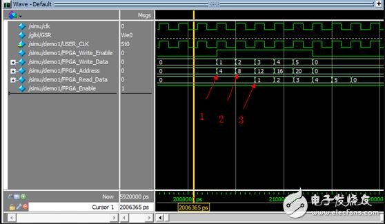
(Fig. 4.1)
The program prepares the address and the data to be written to the RAM at 1 o'clock, and writes it to the RAM at 2 o'clock. At 3 o'clock, the port outputs the data written to the RAM at 2 o'clock, which is slightly different from the picture of PG058.
(Figure 4.2)
4. PostscriptRegarding BRAM, I recommend a youtube video that is very clear and easy to understand.
What is a Block RAM in an FPGA?
Others Patent Vape,Air Bars Disposable,Disposable Vapor Pen,Disposable E-Cigarette
Guangzhou Yunge Tianhong Electronic Technology Co., Ltd , https://www.e-cigaretteyfactory.com