
I know that I am fascinated by everything related to electronics, but from any point of view, today's field-programmable gate arrays (FPGAs) are all "outstanding" and really great devices. If in this era of intelligence, in this field, you want to have a skill, you have not paid attention to FPGA, then the world will abandon you, the era will abandon you.
The high-speed system PCB design considerations associated with SERDES applications are as follows:
(1) Microstrip and Stripline wiring.
The microstrip line is the wiring on the outer signal layer of the reference plane (GND or Vcc) separated by a dielectric, which minimizes the delay; the strip line is the inner signal between the two reference planes (GND or Vcc) Layer wiring, which allows for greater capacitive reactance, easier impedance control, and cleaner signal as shown.
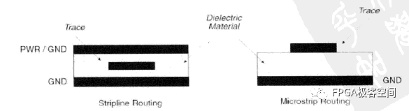
Microstrip and stripline optimal routing
(2) High-speed differential signal pair wiring.
Common methods for high-speed differential signal-to-wiring are edge-coupled (micro-band) (edge), edge-coupled stripline (embedded signal layer, suitable for high-speed SERDES differential signal pairs), and Broadside-coupled microstrip. Shown.
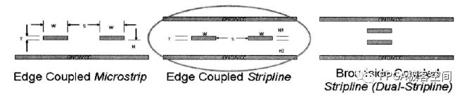
High speed differential signal pair wiring
(3) Bypass capacitor (BypassCapacitor).
The bypass capacitor is a small capacitor with a very low series impedance. It is mainly used to filter out high frequency interference in high speed converted signals. There are three types of bypass capacitors used in FPGA systems: high-speed systems (100MHz~1GHz), commonly used bypass capacitors range from 0.01nF to 10nF, generally within 1cm from Vcc; medium-speed systems (10MHz/100MHz) Commonly used bypass capacitors range from 47nF to 100nF tantalum capacitors, generally within Vcc 3cm; low-speed systems (below a few megahertz), commonly used bypass capacitors range from 470nF to 3300nF capacitors, which are relatively freely laid out on the PCB.
(4) Optimal wiring of the capacitor.
Capacitor wiring can follow the following design guidelines as shown.
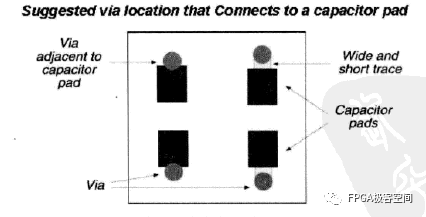
Capacitor optimal wiring
Use a large via (Via) to connect the capacitor lead pads to reduce coupling capacitance.
Use a short, wide wire to connect the vias of the vias and capacitor pins, or connect the pads of the capacitor pins directly to the vias.
Use LESR capacitors (Low Effective Series Resistance).
Each GND pin or via should be connected to ground plane.
(5) High-speed system clock wiring points.
Avoid using sawtooth windings and clock wiring as straight as possible.
Try to route on a single signal layer.
Do not use vias as much as possible because the vias will cause strong reflections and impedance mismatches.
Try to use microstrips on the top layer to avoid over-holes and minimize signal delay.
Place the ground plane as close as possible to the clock signal layer to reduce noise and crosstalk. If you use the internal signal layer to route the clock line, you can use two ground planes to sandwich the clock signal layer to reduce noise and interference. Reduce signal delay.
The clock signal should be properly impedance matched.
(6) High-speed system coupling and wiring considerations.
Note the impedance matching of the differential signals.
Pay attention to the width of the differential signal line so that it can tolerate 20% signal rise or fall time.
With a suitable connector, the connector should be rated for the highest frequency of the design.
The differential signal pairs are coupled as far as possible using the edge-couple method, avoiding the use of broadside-couple coupling, and using the 3S fractional rule to avoid over coupling or crosstalk.
(7) Precautions for high-speed system noise filtering.
Reduce the low frequency interference caused by power supply noise (below 1KHz), and add shielding or filtering circuit to each power supply access terminal.
Add 100F electrolytic capacitor filter to each place where the power supply enters the PCB.
To reduce high frequency noise, decoupling capacitors are placed as much as possible at each of Vcc and GND.
Place the Vcc and GND planes in parallel and separate them with a dielectric (such as FR-4PCB) and place bypass capacitors on the other layers.
(8) High-speed system ground bounce (Ground Bounce)
Try to add a decoupling capacitor to each Vcc/GND signal pair.
An external Buffer is added to the output of a high-speed flip signal such as a counter to reduce the drive capability.
The user I/O used is set to an output signal that is output low, which is equivalent to a virtual GND that connects these low level outputs to the ground plane.
The output signal with less demanding speed is set to the mode of Slow Slew.
Control load capacitance.
Reduce the signal that the clock is constantly flipping, or distribute this signal as evenly as possible around the chip.
Route the frequently flipped signal as close as possible to the GND pin of the chip.
When designing synchronous timing circuits, you should try to avoid all transients of the output.
The power supply and the ground are placed apart so that the inductance can be neutralized as a whole.
Universal Meter,Multi-Function Multimeter,Electronic Multimeter,Electronic Volt-Ohm-Ma Meter
YINTE TOOLS (NINGBO) CO., LTD , https://www.yinte-tools.com