This circuit based on cross-coupled hot cathode tubes was invented by American scientist OH Schmitt. Since then, Schmitt triggers have become an important building block in many signal processing circuits. The hysteresis—the difference between the high voltage and low voltage thresholds—is an inherent characteristic of Schmitt trigger operation. When the input signal crosses these two thresholds, the circuit can reject the noise contained in the input signal and produce a rectangular output signal with the same frequency as the input signal.
Whether you implement a Schmitt trigger with a transistor, an op amp, or a comparator, you need to determine the required hysteresis and what the two threshold voltages are. If you know the magnitude of the input signal and the amount of noise it may contain, then this question is easy to answer. However, if these parameters are variable or largely unclear, it is tricky to set thresholds to produce reliable triggers: too large hysteresis may not allow the input signal to cross one or two of the thresholds. A too small hysteresis voltage can cause false triggering if the input signal has a lot of noise.
The design example shown in Figure 1 can solve these problems. The implementation circuit shown in the figure can automatically adjust the trigger threshold based on the amplitude of the input signal. Comparator IC1A and analog switch IC2B and capacitor C1 form a positive peak detector. When the input signal rises above the voltage stored in C1 at the inverting input of the comparator, the comparator output will go high, which in turn causes IC2B to switch to the position shown in the schematic. The detector now samples the input signal and fills the charge stored in C1. When the input signal drops below the voltage on C1, the switch will change state and the voltage VU stored in C1 becomes the DC level corresponding to the positive peak of the input signal.
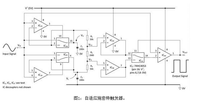
Comparator IC1B, analog switch IC2C and capacitor C2 form a negative peak detector. It works in the same way as the forward peak detector described above, except that the sample is the negative peak of the signal, so the voltage VL stored in C2 is the DC level corresponding to the negative peak of the input signal.
A resistor network composed of R1, R2, and R3 provides a discharge path for the charge stored in the sampling capacitor, and sets an upper threshold voltage VTU and a lower threshold voltage VTL for the last comparator IC4A, respectively. The selection of the resistance value is such that the VTU is slightly smaller than VU and the VTL is slightly larger than VL. If R1=R3 is set, the voltage difference calculated as a percentage is equal to:
Voltage difference = [R1/(2R1+R2)] × 100%
If the component values ​​shown in the figure are used, the VTU is 5% smaller than VU, and the VTL is 5% larger than VL. In this way, the threshold can be continually adjusted to track the input signal amplitude and DC level. For example, a signal superimposed on a 2V DC level with a peak-to-peak value of 1V (ie, VU=2.5V, VL=1.5V) would result in a threshold of VTU=2.45V and VTL=1.55V. It can be seen that the hysteresis voltage VH (0.9V in this example) given by VH=VTU-VTL is always slightly lower than the peak-to-peak value of the input signal amplitude.
The threshold voltage is buffered by IC3A and IC3B and fed into analog switch IC2A. To understand how the last part of the circuit works, it can be assumed that IC2A is in the state shown in the figure, so the threshold voltage VTU is fed to the inverting input of the comparator, and the input signal of the comparator non-inverting input rises from the negative peak. The digital output signal VOUT is currently at a low level. At the moment the input signal just crosses the VTU, the comparator output goes high immediately, causing IC2A to change state and feed the VTL to the inverting input of the comparator. This positive feedback—typical Schmitt trigger behavior—enses a fast, complete switch of the digital output signal. Buffers IC3A and IC3B are necessary (especially at high frequencies) to prevent stray capacitance at the inverting input of IC4A from causing distortion of the VTU and VTL when IC2A changes state.
The oscilloscope waveforms of Figures 2 and 3 show the performance of the test circuit built using comparator IC1 and IC4 = TLC3702 and op amp IC3 = TLC2272. These rather extreme examples reflect the ability of the circuit to handle very different input signals.
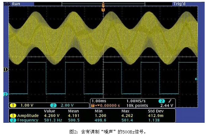

In Figure 2, the source signal is a 500Hz sine wave signal with a peak-to-peak value of 1.56V modulated by a 100kHz sine wave with a peak-to-peak value of 2.88V. Finally, it is superimposed on a 2.5V DC level with a peak-to-peak value of about 4.4. The composite signal of V. Although the "noise" amplitude is almost twice the amplitude of the source signal, the circuit output can still be switched on and off at the source signal frequency and is completely unaffected by high frequency modulation. Figure 3 shows the response of the circuit to very small input signals. The source signal here is a 100 kHz sine wave superimposed on a DC level of 400 mV with a peak-to-peak value of approximately 30 mV. The presence of a switch glitch in the input signal (caused by a less than perfect breadboard layout) can cause some jitter in the output signal. Note: The input signal in Figure 2 is more than 100 times larger than the signal in Figure 3. In fact, if the input signal remains within the common-mode range of the comparator and buffer (about 0 to 4V in this case), the circuit can handle different signal amplitudes that vary in amplitude by two orders of magnitude. AC coupling is only required when the signal DC level is outside the input common mode range.
You should choose C1 and C2 to accommodate the expected frequency range. A value of around 100 nF is suitable for frequencies above or below about 300 Hz. When less than this frequency, the sampling capacitor should be increased to prevent excessive attenuation ripple on VU and VL. The TLC3702 comparator works well to around 100kHz, but beyond this level you may need to choose a faster device. The above circuit is not suitable for all trigger applications, but is useful for applications where the fixed threshold of a conventional Schmitt trigger is not suitable.
High efficient charging speed for Toshiba laptop, stable current outlet can offer power for the laptop at the same time charge the laptop battery. The best choice for your replacement adapter. We can meet your specific requirement of the products, like label design. The plug type is US/UK/AU/EU. The material of this product is PC+ABS. All condition of our product is 100% brand new.
Our products built with input/output overvoltage protection, input/output overcurrent protection, over temperature protection, over power protection and short circuit protection. You can send more details of this product, so that we can offer best service to you!
Toshiba Adapter,Adapter For Toshiba,Power Supply For Toshiba,Laptop Charger For Toshiba
Shenzhen Waweis Technology Co., Ltd. , https://www.waweis.com