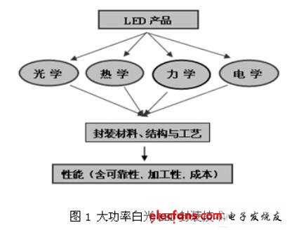
High-power LED packaging mainly involves light, heat, electricity, structure and process, as shown in Figure 1. These factors are independent of each other and affect each other. Among them, light is the purpose of LED packaging, heat is the key, electricity, structure and process are the means, and performance is the specific embodiment of the packaging level. From the perspective of process compatibility and reduction of production cost, LED package design should be carried out simultaneously with chip design, that is, the package structure and process should be considered in chip design. Otherwise, after the chip manufacturing is completed, the chip structure may be adjusted due to packaging requirements, thereby prolonging the product development cycle and process cost, and sometimes even impossible.
Specifically, the key technologies of high-power LED packaging include:
1. Low thermal resistance packaging process
For the existing LED light efficiency level, since about 80% of the input electric energy is converted into heat, and the LED chip area is small, chip heat dissipation is a key problem that the LED package must solve. Mainly include chip layout, packaging material selection (substrate material, thermal interface material) and process, heat sink design, etc.
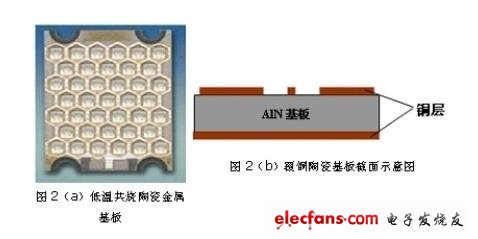
LED package thermal resistance mainly includes internal thermal resistance and interface thermal resistance of materials (heat dissipation substrate and heat sink structure). The function of the heat dissipation substrate is to absorb the heat generated by the chip and conduct it to the heat sink to achieve heat exchange with the outside world. Commonly used heat-dissipating substrate materials include silicon, metals (such as aluminum, copper), ceramics (such as AlN, SiC), and composite materials. For example, Nichia ’s third-generation LED uses CuW as the substrate, and the 1mm chip is flip-chip mounted on the CuW substrate to reduce the thermal resistance of the package and improve the luminous power and efficiency; Lamina Ceramics has developed a low-temperature co-fired ceramic metal substrate , As shown in Figure 2 (a), and developed the corresponding LED packaging technology. This technology first prepares high-power LED chips and corresponding ceramic substrates suitable for eutectic welding, and then directly welds the LED chips and the substrate together. Because the eutectic solder layer, electrostatic protection circuit, drive circuit and control compensation circuit are integrated on the substrate, not only the structure is simple, but also because of the high thermal conductivity of the material and few thermal interfaces, the heat dissipation performance is greatly improved, and it is packaged for high-power LED arrays Proposed a solution. The high thermal conductivity copper-clad ceramic board developed by the German Curmilk company is formed by sintering the ceramic substrate (AlN or) and the conductive layer (Cu) at high temperature and high pressure, without using a binder, so it has good thermal conductivity, high strength and strong insulation , As shown in Figure 2 (b). Among them, the thermal conductivity of aluminum nitride (AlN) is 160W / mk, and the thermal expansion coefficient is (equivalent to the thermal expansion coefficient of silicon), thereby reducing the thermal stress of the package.
Studies have shown that the package interface also has a great influence on the thermal resistance. If the interface cannot be handled correctly, it is difficult to obtain good heat dissipation. For example, an interface with good contact at room temperature may have an interface gap at high temperature, and warpage of the substrate may also affect bonding and local heat dissipation. The key to improving LED packaging is to reduce the thermal resistance of the interface and interface contact and enhance heat dissipation. Therefore, the selection of the thermal interface material (TIM) between the chip and the heat sink substrate is very important. Commonly used TIMs for LED packaging are conductive adhesives and thermally conductive adhesives. Due to their low thermal conductivity, they are generally 0, 5-2, and 5 W / mK, resulting in high interface thermal resistance. The use of low-temperature or eutectic solder, solder paste, or conductive paste doped with nanoparticles as the thermal interface material can greatly reduce the interface thermal resistance.
Second, the high light extraction rate packaging structure and process
During the use of LEDs, the loss of photons generated by radiation recombination when emitted outwards mainly includes three aspects: internal structural defects of the chip and the absorption of materials; the reflection loss of photons at the exit interface due to the difference in refractive index; and due to The total reflection loss caused by the incident angle being greater than the critical angle of total reflection. Therefore, a lot of light cannot exit from the chip. By coating a transparent adhesive layer (potting compound) with relatively high refractive index on the chip surface, the adhesive layer is located between the chip and the air, thereby effectively reducing the loss of photons at the interface and improving the light extraction efficiency. In addition, the role of potting glue also includes mechanical protection of the chip, stress relief, and as a light guide structure. Therefore, it is required to have high light transmittance, high refractive index, good thermal stability, good fluidity and easy spraying. In order to improve the reliability of LED packaging, the potting compound is also required to have characteristics of low moisture absorption, low stress, and aging resistance. Currently commonly used potting adhesives include epoxy resin and silicone. Because of its high light transmittance, large refractive index, good thermal stability, low stress, and low hygroscopicity, silica gel is significantly better than epoxy resin, and is widely used in high-power LED packaging, but the cost is higher. Studies have shown that increasing the refractive index of silica gel can effectively reduce the photon loss caused by the physical barrier of the refractive index and improve the external quantum efficiency, but the performance of silica gel is greatly affected by the ambient temperature. As the temperature increases, the thermal stress inside the silica gel increases, resulting in a decrease in the refractive index of the silica gel, thereby affecting the LED light efficiency and light intensity distribution.
The role of phosphors is to combine light and color to form white light. Its characteristics mainly include particle size, shape, luminous efficiency, conversion efficiency, stability (thermal and chemical), etc. Among them, luminous efficiency and conversion efficiency are the key. Studies have shown that as the temperature rises, the quantum efficiency of the phosphor decreases, the light output decreases, and the radiation wavelength also changes, causing changes in the color temperature and chromaticity of the white LED. Higher temperatures will also accelerate the aging of the phosphor. The reason is that the phosphor coating is made of epoxy or silica gel and phosphor powder, and the heat dissipation performance is poor. When exposed to violet or ultraviolet light, it is prone to temperature quenching and aging, which reduces the luminous efficiency. In addition, the thermal stability of encapsulants and phosphors at high temperatures is also problematic. Because the size of commonly used phosphors is above 1um, the refractive index is greater than or equal to 1,85, while the refractive index of silica gel is generally around 1,5. Due to the mismatch in refractive index between the two, and the size of the phosphor particles is much larger than the light scattering limit (30nm), there is light scattering on the surface of the phosphor particles, reducing the light extraction efficiency. By incorporating nano-phosphor powder into silica gel, the refractive index can be increased to above 1, 8 to reduce light scattering, improve the LED light output efficiency (10% -20%), and can effectively improve the quality of light color.
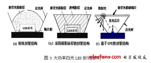
The traditional phosphor coating method is to mix the phosphor with potting glue, and then apply the dot on the chip. Since the coating thickness and shape of the phosphor cannot be accurately controlled, the color of the outgoing light is inconsistent, and blue or yellow light appears. The Conformal CoaTIng technology developed by Lumileds Co., Ltd. can achieve the uniform coating of phosphors, ensuring the uniformity of light color, as shown in Figure 3 (b). However, research shows that when the phosphor is directly coated on the surface of the chip, the light extraction efficiency is low due to the existence of light scattering. In view of this, the American Rensselaer Institute has proposed a photon scattering extraction process (Scattered Photon ExtracTIon method, SPE). By arranging a focusing lens on the surface of the chip and placing the glass sheet containing the phosphor at a certain distance from the chip, not only Improve the reliability of the device, and greatly improve the light efficiency (60%), as shown in Figure 3 (c).
In general, in order to improve the light extraction efficiency and reliability of LEDs, the encapsulation layer is gradually replaced by high refractive index transparent glass or glass ceramics. The uniformity of the phosphor powder also improves the packaging efficiency. In addition, reducing the number of optical interfaces in the light exit direction of the LED is also an effective measure to improve the light output efficiency.
The energy management system accesses a variety of energy consumption collection interruptions through the network, and implements centralized monitoring, measurement and management of data of various energy varieties. With multidimensional energy consumption statistics and dynamic trend analysis, it helps users to master the energy consumption situation, analyze and diagnose the energy efficiency level, identify the key points of energy saving, analyze the energy-saving potential, and point out the direction for enterprises to improve energy utilization efficiency.
Energy Management System,Energy Management Software Integrateion,Energy Managment Software,Integrateion Energy Management Software
Jiangsu Sfere Electric Co., Ltd , https://www.elecnova-global.com