The data acquisition system based on Sigma-Delta ADC sampling has been mentioned in the previous blog post, and the design method of Sinc3 sampling filter is described in detail, which is described in detail. Later, the previous ADC was also made into a PCB board, which formed a complete FPGA-based Sigma-Delta data acquisition system.
From the perspective of modulator coding theory, most traditional analog-to-digital converters are of the Linear Pulse Code Modulation (LPCM) type, such as parallel comparison type and successive approximation type. This type of analog-to-digital converter is quantized according to the magnitude of the signal. An ADC with a resolution of n can divide its range into 2 different power levels of n, and achieve a different nth power of 2 The quantization level requires a fairly complex resistor (or capacitor) network and high precision analog electronics. As the number of bits n increases, the implementation of the comparison network becomes more and more difficult, thus limiting the resolution of the analog to digital converter. At the same time, factors such as integration and temperature changes have an impact on high-precision analog electronics, further limiting the resolution of the converter.
Unlike a conventional LPCM ADC, the ADC does not directly quantize the signal according to the amplitude of the signal, but quantizes the difference between the previous sample value and the latter sample value (ie, increment), in a sense It is quantized and encoded according to the envelope shape of the signal. Δ in the ADC name indicates an increment, and Σ indicates integration or summation. Because the ADC uses a very low-order quantizer (usually 1 bit), it avoids the difficulties faced by the LPCM ADC in manufacturing, and is suitable for the implementation of semiconductor manufacturing technology. On the other hand, because of its extremely high sampling rate and modulation technology, extremely high resolution can be achieved. Because it uses low bit quantization, it is not as sensitive to the amplitude variation of the input signal as the LPCM type ADC. Compared to traditional LPCM-type ADCs, ADCs use a high sampling rate in exchange for high-order quantization to improve resolution.
The sampling circuit is composed as shown in Figure 1. It consists of an RC filter circuit, a modulator, a photocoupler, and an FPGA (digital filter).
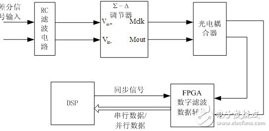
Figure 1 Block diagram of the entire system
The input differential analog signal at the front end of the sampling circuit is filtered by a first-order filter circuit and then enters the modulator. The modulator converts the differential analog signal into a high-low level bit stream signal synchronized with the clock signal. The output clock signal Mclk and the bit stream signal Mout have two processing modes, one is directly into the FPGA after being isolated by the optocoupler, and the method is suitable for the occasion that the analog signal transmission distance is relatively short; the other is the clock signal Mclk and The bit stream signal Mout is converted into an optical signal, which is transmitted to the FPGA end by optical fiber, and then converted into an electrical signal into the FPGA. This method can transmit the analog signal over a long distance, so that the analog signal is not interfered. After receiving the signal, the FPGA internally filters the signal with the Sinc3 filter, converts the filtered result into serial data, transmits the sampled value to the DSP by asynchronous serial communication, or converts the filtered result into parallel data transmission. DSP.
The Sigma-Delta ADC chip selected here is from the ADS1205 manufactured by Texas Instruments. This device is a 2nd-order high-performance Sigma-Delta modulator with CMOS technology and 16-bit resolution and 14-bit resolution. Linearity, the internal crystal is 20MHz, but the actual operating frequency is 10MHz after 20MHz divided by 2, it can be either differential input or single-ended input. We mainly use the signal acquisition in the motor control system, so as long as the single-ended input.
The system hardware can be roughly divided into two parts. The first half mainly implements Sigma-Delta modulation of analog signals to obtain 10MHz 0-bit stream digital signals. This part mainly uses ADS1205 chip for Sigma-Delta modulation; second-order Sigma-Delta modulation The resulting signal is actually a 1,0 bit stream with a duty cycle that varies with the magnitude of the analog input voltage. One of the ratios is proportional to the magnitude of the analog input voltage. The general difference is that this bit stream signal has a very high speed due to oversampling, so the focus is on how to reduce it to the appropriate speed when the filter is in use. The latter part mainly implements digital filtering. The integral part of this filter still works below the oversampling frequency. It only extracts the system frequency by 32 frequency division in the comb part, so the output result is downsampled, and finally the high speed A 0, 1 stream signal is converted to a lower speed 14-bit digital signal for subsequent digital processing systems, because this design is based on FPGA-based digital filtering, and the hardware design has chosen Red Hurricane II - Xilinx RCIISP3S400 because It has a digital tube that can be easily displayed. On this development board, some program-assisted verification hardware designs were also written in Verilog HDL language, and digital tubes were used as displays. Because the number of bits (only 4 digits) is limited, only the first three decimal digits are outputted during verification, that is, two digits after the decimal point are added, plus one digit, and the test site and several test results are tested. as shown in picture 2.
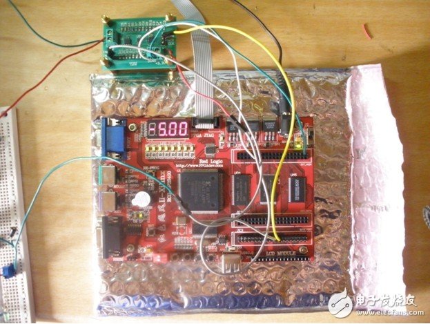
Figure 2 Experimental device and digital tube display
In order to check the effect of the measurement method, the output current was tested on a two-level inverter with an output frequency of 5 Hz and a sampling frequency of 1 kHz. The measurement experiment waveform is shown in Figure 2. The specific test method is to first send an arbitrary waveform signal of -5 to +5V to the Sigma-Delta ADC for sampling, and then the Sigma-Delta ADC sends the data to the FPGA for sampling filtering; the FPGA transmits the filtered result to the SPI protocol to the SPI protocol. TI's TMS320F28335 DSP finally uses the DAC7724U DAC to output the waveform to the oscilloscope (because it is not familiar with the DAC chip directly controlled by the FPGA, so using this stupid way, the DSP directly writes the IO space, how can the FPGA be made?) .
The CH1 channel is the waveform output by the Hall sensor (produced by LEM), and the CH2 channel is the waveform measured by the measurement method. It can be seen that the function of the whole system is effective and resistant to noise.
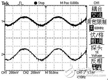
Figure 3 DA output test results
Guangzhou Winson Information Technology Co., Ltd. , https://www.barcodescanner-2d.com