With the improvement of processing efficiency, memory density and system integration, embedded vision has gradually expanded from the traditional to the emerging application field, and the market scale will increase significantly within ten years. With the increasing diversity of application fields, the imaging sensor system is becoming more complex when it is being developed.
Vision systems are becoming more and more popular in various industries and applications, and even an example of an embedded vision system that is carried by a smart phone every day. These devices not only perform image capture and image recording, but also perform applications that augment virtual reality. This shows that embedded vision technology has a very high degree of acceptance.
With the improvement of processing efficiency, memory density and system integration, embedded vision has gradually expanded from the traditional to the emerging application field (Figure 1). This makes embedded vision widely accepted among consumers, industry and government, and there must be significant growth in ten years.
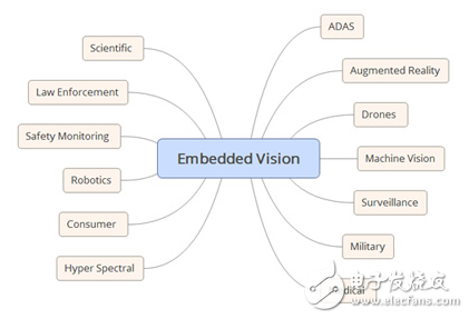
Figure 1 Common embedded vision applications. 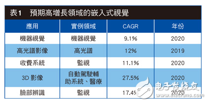
Table 1 lists some of the areas in the rise of embedded visuals, some of which are obvious and some of which are not obvious.
Basic concept of embedded visionThe so-called embedded vision system contains the entire signal chain that receives photons from the selected image sensor to the system output. The processed or unprocessed image or information is captured from the image at the receiving end and provided to the downstream system, and the embedded system architect is responsible for ensuring the performance of the output process is received according to system requirements.
Therefore, embedded vision system architects need to be familiar with the various concepts and technologies associated with sensors and post-processing systems. Designed for beginners, this article is designed to give readers a basic understanding of the technology and concepts.
First, we must be familiar with the electromagnetic spectrum and the spectral domain in which the system is expected to operate, because the spectrum that is discernible by the naked eye is only between 390 nm (blue) and 700 nm (red), and is also the visible spectrum; depending on the choice of imaging equipment, We are able to capture a wider range of wavelength images including X-rays, UV, IR, and visible spectrum.
For near-infrared light and below, we can use charge-coupled components (CCD) or complementary metal-oxide-semiconductor (CMOS1) image sensors (CIS); in the infrared spectrum, a dedicated infrared detector is required. Infrared spectroscopy requires a dedicated sensor, in part because chip imaging sensors such as CCD or CIS require excitation energy. These components typically require 1 eV of photon energy to excite an electron. However, in the infrared spectral range, the photon energy is between 1.7 eV and 1.24 meV, so the infrared image sensor should be based on HgCdTe or InSb. These low-energy sensors are often used in conjunction with CMOS read ICs (ROICs) to facilitate sensor control and reading.
The two most common sensor technologies are CCD and CIS:
. The charge-coupled component (CCD) is considered the best simulation component, so if you need to integrate with a digital system, you need to add ADC and frequency generation function under a certain analog voltage. Each pixel stores the charge generated by the photons, and most applications are arranged in rows by a 2D array, each row consisting of multiple pixels. When reading the CCD, it is necessary to transfer each line in parallel to the read buffer through the line-to-row transfer, and then read each line serially through the read buffer. This buffer converts the charge into a voltage during the reading process.
. CMOS image sensors enable tighter integration of the ADC, bias, and driver circuitry on the same chip, dramatically reducing system integration requirements while increasing the complexity of CIS design. Active pixel sensor (APS) is the core of CIS, which differs from CCD in that each pixel of CIS contains a set of photodiodes and read amplifiers at the same time, and can read any pixel in the array separately.
Although most embedded visions use CIS components, CCD is still the main sensor used in high-end scientific research applications. The content mentioned in this article applies to CIS or CCD imaging technology.
Resolution is the primary consideration for sensor selectionUsers must have a deep understanding of the system in order to select the correct image sensor. The following points are considered:
First, the user must decide what resolution is required, that is, determine the amount of pixels that must be included in each line, and how many lines the detector needs. For example, in the case of astronomical science applications, high-resolution 2D components are likely to be used, but in industrial imagery imaging applications, only linear scanning may be required.
The linear scan component consists of a single row of pixels on the X-axis, which is often used for moving camera or target applications to generate an image of the Y-axis. Typically such sensors are used to verify application or optical character recognition (OCR). Some areas require time-domain integration (TDI) linear scanning sensors, which consist of multiple lines on the X-axis and move with the target; pixels move from one to the next, along with the charge over time. Integration for more sensitive detection.
However, TDI needs to synchronize between line-to-row and target movements to prevent blurring and image defects. Since only a few lines need to be read, the frame rate can be quite high.
A 2D array contains multiple rows of pixels, and the array size determines the maximum frame rate of the sensor. Usually in order to achieve a higher frame rate, the 2D component reads multiple pixels in parallel. In addition, the 2D component can also perform window operations (also known as regions of interest, ROI) and read specific regions of interest to achieve higher frame rates. These components can be used in a wide range of applications, and the information is contained in 2D images such as Advanced Assisted Driving Systems (ADAS), surveillance or scientific research.
After determining the format of the image sensing and the required resolution, it is necessary to consider the "pixel pitch". Because it determines the size of the pixel, and this is related to how much charge generated by the incident photons can be collected. Therefore, a smaller pixel pitch means that less charge can be collected during one integration cycle (the time the sensor is exposed to the image). If the pixel pitch is small, it means that capturing images requires a longer integration time, which affects the ability of the sensor to capture images in fast motion and reduces the performance of low-light photos.
High Frequency Flyback Transformer
RM10 electrical transformer,EE13 high frequency transformer,EE10 LED transformer,EE16 flyback transformer
IHUA INDUSTRIES CO.,LTD. , https://www.ihuagroup.com