The S6BP203A is a single-channel buck-boost DC/DC converter IC with four built-in switching FETs. The IC is capable of delivering up to 2.4A of load current over a wide input voltage range of 2.5V to 42V. The IC has an operating mode that automatically changes to PFM operation under low load conditions, resulting in ultra-high efficiency and ultra-low quiescent current of 50μA. It provides a stable output voltage with a transition time of 1ms. Therefore, the IC is suitable for use as a power solution for automotive and industrial applications.
The IC has a SYNC function that selects SYNC_IN that can input an external clock signal. When an external clock signal of 200 kHz to 400 kHz is input, the FET performs a switching operation by a synchronization signal from an external clock. When the external clock signal is not input, the FET performs a switching operation from the internal clock. The internal clock signal from 200kHz to 2.1MHz can be set by an external resistor. Since the IC does not require an external voltage setting resistor and a phase compensation capacitor, it reduces the number of components and reduces the component mounting area.
The IC has five protection functions, namely input undervoltage lockout (input UVLO), output undervoltage protection (output UVP), output overvoltage protection (output OVP), output overcurrent protection (output OPC) and thermal shutdown ( TSD).
In addition, the IC has a power good (PG) function that indicates the state of the output voltage (VOUT pin).
When the output voltage reaches the PG voltage, the PG signal is output.
Main features of S6BP203A
Wide input voltage range: 2.5V~42V
Output voltage: 3.3V
Wide operating frequency range: 200kHz~2.1MHz
External synchronous clock range: 200kHz~400kHz
SYNC function
SYNC_IN: External clock input
(When an external clock is not input, the IC operates with an internal clock)
Ultra-high efficiency through PFM operation (when the MODE pin is set low)
Automatic PWM/PFM switching operation and fixed PWM operation can be selected through the MODE pin
Built-in switching FET
Synchronous current mode architecture
Shutdown current: less than 1μA
Quiescent current: 50μA
Power good monitor
Monitor output voltage through window comparator
Power-on reset time (settable by factory): 14ms
Soft start time (no load dependency): 0.9ms (when the switching frequency is 2.1MHz)
Enhanced protection
Input undervoltage lockout
Output undervoltage protection: 92.0%
Output overvoltage protection: 108.0%
Output overcurrent protection
Thermal shutdown
Small TSSOP16 package (bare pad): 5mm & TImes; 6.4mm
S6BP203A application
Advanced Driver Assistance System (ADAS)
dash board
Automotive application
Industrial application
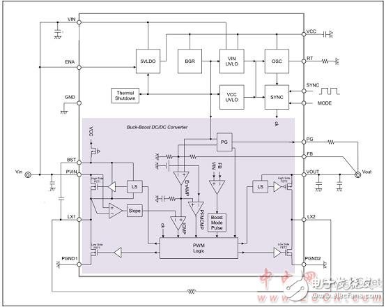
Figure 1 S6BP203A block diagram
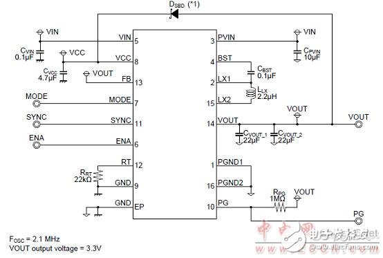
Figure 2 S6BP203A application case circuit diagram
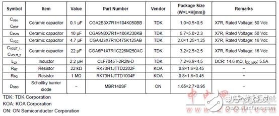
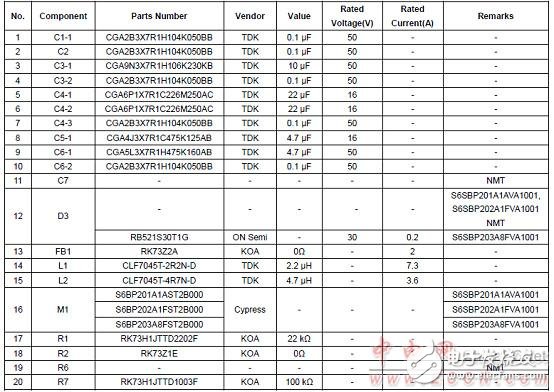
Table 1 S6BP203A application case circuit material list
Automotive PMIC Evaluation Board S6SBP203A8FVA1001
The S6SBP203A8FVA1001 is an evaluation kit for automotive mains modules. The evaluation board implements the power management IC S6BP203A.
The S6BP203A is a single-channel buck-boost DC/DC converter IC with four built-in switching FETs. The IC is capable of delivering up to 2.4A of load current over a wide input voltage range of 2.5V to 42V. The IC has an operating mode that automatically changes to PFM operation under low load conditions, resulting in ultra-high efficiency and ultra-low quiescent current of 50μA. It provides a stable output voltage with a transition time of 1ms. Therefore, the IC is suitable for use as a power solution for automotive and industrial applications.
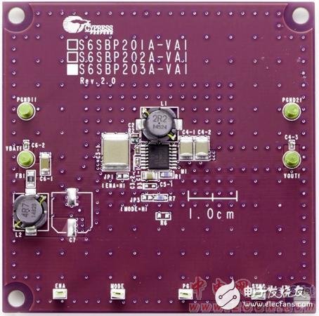
Figure 3 Outline drawing of the car PMIC evaluation board S6SBP203A8FVA1001
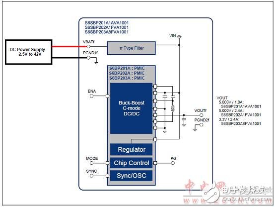
Figure 4 Block diagram of the car PMIC evaluation board S6SBP203A8FVA1001
Table 3 Car PMIC Evaluation Board S6SBP203A8FVA1001 Bill of Materials
Network Accessories,Wifi Adapter,Fiber Optic Network Components,Splitter Fiber Optic
Cixi Dani Plastic Products Co.,Ltd , https://www.dani-fiber-optic.com