 Hong Kong University of Science and Technology (HKUST) has recently developed a high performance silicon-based green yellow nitrogen semiconductor LED. This new research result was published on the IEEE Electronic Device Letters (May 29th). The researchers said that its 565nm yellow LED is the first silicon substrate MQW device.
 In theory, the use of silicon as a substrate can reduce material costs and economies of scale for mass production of large wafer-diameter products, but compared to traditional, more expensive stand-alone GaN, sapphire, or silicon carbide (SiC) substrates, Silicon substrate nitrogen semiconductors lead to greater lattice mismatch. Researchers say that the production of nitrogen semiconductor LEDs with larger wavelengths is challenging because it is difficult to produce indium gallium nitride (InGaN) products with good quality and higher indium concentrations. Although the silicon substrate process in the field of semiconductor transistors has been very mature, similar growth methods have recently been applied to LED device materials.
On 2-inch wafers, the researchers used metal-organic vapor deposition (MOCVD) technology to generate the original template, which was nucleated by aluminum nitride (AlN), and eight pairs of aluminum nitride/gallium nitride (AlN/GaN). The layers were composed to create a superlattice (SL) (used as a stress-balanced sandwich) and a 2 μm GaN buffer layer. The researchers first precipitated the SiO2 layer and the indium tin oxide (ITO) layer, then etched the ITO using a hydrogen chloride (HCL) acid solution, and finally used a plasma etching method to form silicon dioxide (SiO2) nanorods. The nanorods have a density of 2x10⁹/cm2 and a surface coverage of 35%. As a mask for GaN regrown, the nanorods can reduce dislocation density and improve crystal quality.
Subsequently, an LED structure was generated by MOCVD technology to generate 800 nm GaN around nanorods, AlN/GaNSL interlayers, 2 μm N-type GaN, 5-period multi-quantum wells (MQWs), and 200 nm p-GaN. The resulting GaN dislocation density is 8x10⁸/cm2, which is referred to as "one of the lowest GaN dislocation densities on the silicon substrate."
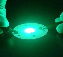
The researchers then prepared materials suitable for emitting yellow (565 nm) and green (505 and 530 nm) light to make 300 μm x 300 μm LED chips. As expected, as the wavelength increases, the light output power (LOP) gradually decreases (Figure 2). At 20 mA, the output power at the 505 nm wavelength is 1.18 mW, and the output power at the 530 nm and 565 nm wavelengths is 0.30 mW and 74 μW, respectively. For 505nm, 530nm, and 565nm devices, the optical output power is saturated at 7.60mW (200mA), 2.72mW (180mA), and 0.52mW (160mA), respectively.
It is said that this is the first time that people have successfully manufactured 565nm yellow InGaN/GaN MQW LEDs on a silicon substrate, and the 505nm LED has much higher LOP than the previous silicon LED devices. In addition to improving material quality, the agency researchers believe that nanorods can also enhance the light extraction scattering effect.
Digital Printing Graphic Overlay
Digital Printing Graphic Overlay,Membrane Switches Graphic Overlays,Membrane Switch Panels ,Membrane Switch Button
CIXI MEMBRANE SWITCH FACTORY , https://www.cnjunma.com