In many tourist attractions and exhibition halls, although visitors can see the exhibits, there are many exhibits, but the information they know is very small. Basically, they should rely on the guides to explain. Due to the lack of guides and cost issues, most of the audience can only watch the flowers and the quality of the exhibition is not high. Therefore, a self-guided tour guide system based on RFID (radio frequency identification technology) and speech synthesis is proposed.
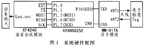
1 Working principle of self-service voice explanation system The self-service voice explanation system consists of two parts: RFID electronic tag and handheld terminal. Handheld terminals mainly include AT89S8252 single-chip microcomputer, non-contact IC card reading and writing and RF module circuit, Keda Xunfei XF-S4240 voice synthesis module, power supply circuit, etc. The main block diagram of the schematic diagram is shown in Figure 1. When the handheld terminal detects the RFID electronic tag, an interrupt is generated and the electronic tag information is read. The exhibit code can be identified, the voice explanation text of the exhibit stored in the single chip microcomputer is called, and the voice synthesis circuit is output through the voice synthesis module to complete the explanation task.
This article refers to the address: http://
2 system hardware design
2.1 Non-contact RF card reader Because the contactless IC card has no contact with the card reading device, it acquires energy and exchanges data from the reading and writing device through RF electromagnetic induction. The read and write operations only need to put the card in the reading and writing. Data exchange and identification can be realized within a certain distance near the device. It is convenient and fast to use and is not easily damaged. It is widely used in places with frequent access and high reliability.
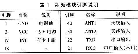
This system is implemented by the WM-01TA module of Beijing Perfect Company. The module is equipped with a loop antenna with an operating frequency of 125 kHz; it has an asynchronous serial communication UART interface; the default serial port baud rate is 9 600 b/s, no parity, 8 data bits, 1 stop bit; readable The EM read-only sensor has a card reading distance of 60 to 90 mm, a card reading speed of more than 0.5 s, and a standard IC pin DIP40 form factor for easy insertion into the target board. The RF module has a total of 7 pins, the pin description is shown in Table 1. The device is inexpensive and fully meets the design needs of the project.
When the card enters the sensing area, the module sends a card number to the serial port. If the card does not leave the sensing area, the module will not send the card number to the serial port. If the card leaves the sensing area and then enters the sensing area, the module needs to send the card number again.
TTL232 data transmission is mainly the transmission card number, and its transmission data format is: AAH FFH DO D1 D2 D3 D4 checksum, a total of 8 bytes, of which AAH and FFH are command codes: DO to D4 are 40-bit card numbers, of which low address For the high byte Motorola structure: checksum is 0 to 5 bits for a total of 7 bytes of "XOR" XOR value. For example, a 40-digit card number is 01021DF6FA (HEX), and the corresponding transmission format is: AAH FFH 01H 02H 1DH F6H FAH 47H, and its card number is 5 bytes: 01H 02H 1DH F6H FAH.
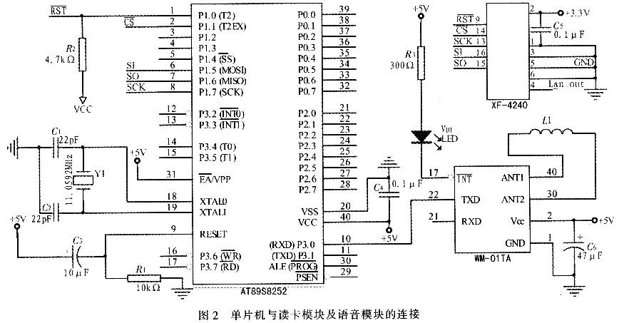
WM-01TA is connected to the MCU through the UART interface, as shown in Figure 2.
2.2 Voice Module XF-S4240
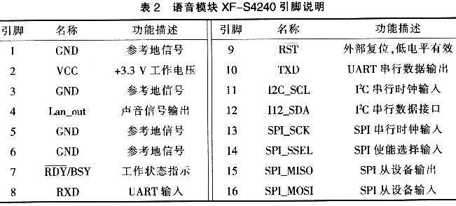
The XF-S4240 Chinese speech synthesis module is an embedded Chinese speech synthesis module launched by Zhongke Daxun Information Technology Co., Ltd. for high-end applications. Can support any Chinese text, English letter synthesis. The module receives the text to be synthesized through asynchronous serial port (UART), SPI interface and I2C bus, and directly synthesizes it into voice output. The module supports four internal code formats such as GB2312, GBK, BIG5, UNICODE, intelligent text analysis processing algorithms, and supports a variety of control commands, including: synthesis, stop, pause synthesis, continue synthesis. The XF-S4240 voice module is packaged into 16 terminals, and the functions of each terminal are shown in Table 2.
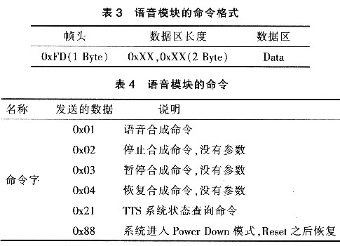
The command format of the voice module is composed of a frame header, a data length area, and a data area. The definition of each part is shown in Table 3. The commands of the voice module are shown in Table 4.
To synthesize "Welcome to visit Mogao Grottoes", simply send the text code in the format GB2312 to the module:
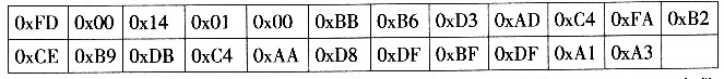
0xFD is the frame header, 0x00 is the high byte of the data area length, Ox14 is the low byte of the data area length (note: the length byte is the synthesized code byte length +2), 0x01 is the speech synthesis command, 0x00 is the GB2312 Command code. 0xBB, 0xB6 are "Happy" GB2312 code, 0xD3, 0xAD is "Welcome" GB2312 code... 0xAD, 0xA3 is "." GB2312 code.
In this design, AT89S8252 and XF-S4240 are realized by SPI communication, and the circuit connection is shown in Figure 2. The voice signal is amplified by the LM386. Since the module is powered by 3.3 V, AMSlll7 is required to convert 5 V to 3.3 V.
2.3 AT89S8252 MCU In the system design, the RF card reader module has a UART interface, and the speech synthesis module has a UART and SPI interface. Since the ordinary 51 single-chip microcomputer has only one serial port, there is a problem of expansion of the serial port. The AT89C8252 MCU is an 8-bit microprocessor from ATMEL. The SPI interface is the main feature of the AT89S8252. It is fully compatible with the 51 MCU, but it is extended on the P1 port (P1.4 to P1.7). SPI interface. It can be easily communicated with the voice module. Therefore, the choice of AT89S8252 in this system can greatly simplify the software and hardware design of the system. ![]() (P1.4): From the enable input pin, active low; MOSI (P1.5): main data output or slave data input pin; MISO (P1.6): main data input or slave data output Pin; SCK (P1.7): Master clock output or slave clock input pin.
(P1.4): From the enable input pin, active low; MOSI (P1.5): main data output or slave data input pin; MISO (P1.6): main data input or slave data output Pin; SCK (P1.7): Master clock output or slave clock input pin.
The AT89S8252 has three SPI registers, the control register SPCR, the status register SPSR, and the data register SPDR.
1) The content format of the control register SPCR is:
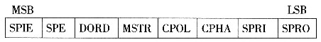
SPIE: SPI Interrupt Enable. When 0, the SPI interrupt is disabled. When it is 1, if the EA is also 1, the SPI interrupt is enabled.
SPE: SPI enable bit. When 0, the SPI channel is disabled; when 1, the SPI interrupt is enabled. At this time, P1.4, P1.5, P1.6, and P1.7 are used as *****, MOSI, MISO, and SCK.
DORO: Data sequence setting bit. When it is 0, the data transmission low bit is first; when it is 1, the data transmission high bit is first.
MSTR: Master-slave mode setting bit. When it is 0, the slave mode is selected; when it is 1, the master mode is selected.
CPOL: Clock polarity setting bit. When 0, the master clock SCK is low when it is not transmitting; when it is 1, SCK is high when it is idle.
CPHA: Clock phase setting bit. This bit, together with CPOL, controls the clock and data relationships between the master and slave devices.
SPRl, SPR0: SPI clock frequency setting bit. These two bits are primarily used for the SCK frequency setting of the master mode device and have no effect on the slave mode device. When it is 00, the frequency is fOSC/4; when it is 01, the frequency is fOSC/16; when it is 10, the frequency is fOSC/64; when it is 11, the frequency is fOSC/128. Here fOSC is the crystal frequency.
In this design, the initialization requires SPIE=0, SPE=l, DORD=O, MSTR=1, CPOL=CPHA=l, SPRl=0, SPR0=1, and the SPI interface can be initialized by the “SPCR=0x5d†statement. .
2) The content format of the status register SPSR is:
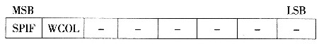
SPIF: SPI interrupt flag bit. This bit is set when a serial transfer is complete. If SPIE and ES are 1, an interrupt is generated. Reading the SPI Status Register SPSR will clear this bit.
WCOL: Write conflict flag. This bit is set when the data register SPDR is written during data transfer. In the data transfer, an error occurs when reading the SPDR register value, and writing to the SPDR register is also invalid. Reading the SPDR register will clear this bit.
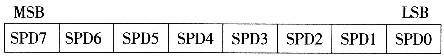
3) The data register SPDR is an 8-bit data bit, and its content format is:
Therefore, the operation of the SPI interface is simple. The subroutine for writing data to the SPI interface is: 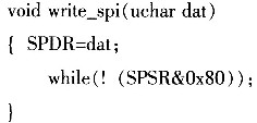
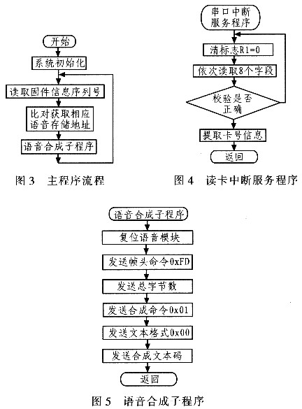
3 System Software Process The software system consists of the main program, the card reader program, and the voice processing program. Among them, the main program completes the initialization of the system (including UART initialization and SPI initialization). If the RF card is close to the antenna, the card reader module sends the TAG information to the MCU through the serial port interrupt. The MCU compares the tag information with the stored card number information, thereby calling the corresponding voice text information and sending it to the XF-S4240 module to play the corresponding voice.
Because the SPI interface is adopted, the communication between the MCU and the voice module is also very simple, and the related codes are as follows: 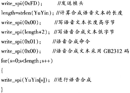
The flow chart is shown in Figures 3 to 5.
4 Conclusion Using AT89S8252 microcontroller and WM-01TA card reader module and XF-S4240 voice module, with antenna module, power module, etc., to achieve a self-service voice explanation system. The system can provide personalized tour guide services in exhibition halls and tourist attractions, which has high practical value.
Guangzhou Yunge Tianhong Electronic Technology Co., Ltd , http://www.e-cigaretteyfactory.com