In general, wireless sensor nodes are sensor-based devices that monitor temperature, humidity, or pressure. Nodes collect data from any type of sensor and then wirelessly pass data to a control unit, such as a computer or mobile device, where it processes, evaluates, and takes action. Ideally, nodes can be powered by energy harvesting mechanisms and become independent devices. In a general sense, the process of energy harvesting is the process of capturing and converting trace energy from light, vibration, or heat into electrical energy.

Figure 1: Example of Energy Collection System Design
Figure 1 shows the block diagram of the energy harvesting system. Energy is collected by energy harvesting systems (such as solar panels) and converted to stable energy by a power management integrated circuit (PMIC), which is then stored using low-leakage, low-impedance capacitors. These energy sources can feed sensor interface loads (such as microcontroller MCUs) to wirelessly transmit sensor data. In this figure, the Energy Harvesting System (EHS) is a wireless sensor node.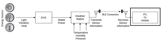
Figure 2: Wireless Sensor Node System Example
Figure 2 shows a block diagram of a wireless sensor node. Here, the processed sensor data is wirelessly transmitted through Bluetooth Low Energy (BLE). BLE is a standard for short-range, low-power wireless applications that apply to communication status or control information. BLE operates in the 2.4 GHz ISM band and Binary Frequency Shift Keying (GFSK) modulation and supports data rates of 1 Mbps.The power management chip (PMIC) is used to stabilize the energy collected by the energy harvesting device and needs to support its own ultra-low power operation. For example, the current consumption of the Cypress S6AE103A PMIC device is as low as 280 nA and the startup power is 1.2 uW (see Figure 3). Therefore, in a low brightness environment of about 100 lx, a small amount of energy can still be obtained from a compact solar panel.
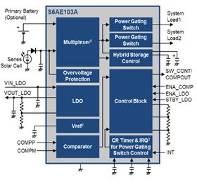
Figure 3: S6AE103A PMIC Device Block Diagram for Energy Harvesting
Efficient Wireless Sensor Node Design <br> Let's consider the steps involved in designing a wireless sensor node:Step 1: Select Hardware:
On the hardware side, you need the right sensors, an MCU that will eventually be powered by an energy harvesting device, and the PMIC. You may need additional passive components, depending on the design.
The sensor can be an analog or digital sensor. Many sensors on the market today use digital sensors based on Integrated Circuit Bus (I2C), Serial Peripheral Interface (SPI), or Asynchronous Transmitter Transmitter (UART) interfaces. Sensors with very low power consumption are also on the market. In order to keep the equipment low-cost and miniaturized, an MCU with integrated BLE can simplify the design and shorten the time to market. To further accelerate design, many vendors use highly integrated, fully-certified programmable modules such as Cypress EZ-BLE Modules. The module consists of a main MCU, two crystals, a chip or board antenna, a housing, and passive components. Since these modules already have the necessary BLE certification, the product can be quickly launched into the market.
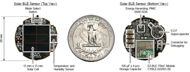
Figure 4: Example of a BLE module - Solar-powered low-power Bluetooth sensor beacon CYALKIT-E02
Step 2: Design Firmware and Estimate Power Consumption <br> After selecting a programmable MCU, the next step is to write the appropriate firmware. The basic functions that the firmware needs to have are the interface for collecting sensor data, the BLE component or stack for transmitting data wirelessly, and the CPU capable of handling the firmware.Since ultra-low consumption operation is the key, the sum of current consumption needs to be taken into account from the beginning. The total energy consumption is the sum of energy consumed by the sensor and the energy consumed by the MCU. Since the sensor usually does not consume too much total energy, the focus should be on how to minimize the energy consumed by the MCU. Before optimizing the current, consider the three main components that consume energy in the MCU: CPU, sensor interface modules (such as I2C, SPI, etc.) and the BLE subsystem. Here, when the radio is on (such as BLE Tx and Rx), the main consumer of energy will be the BLE radio.
Embedded MCUs offer a variety of low-power modes to reduce current consumption. Firmware designers need to consider these low power modes and design codes so that the average current consumption can be minimized. For example, the sensor data is not instantaneously changed, and the firmware needs to scan the sensor data in between (eg every 5 to 10 seconds depending on the sensor). The sensor's read data is wirelessly transmitted via the BLE.
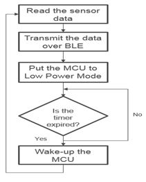
In the case of BLE firmware, sensors can send data along with BLE broadcast packets. We recommend not to transfer too much other data together with the broadcast packet, as this will increase the current further. Between the broadcast interval and the sensor scan interval, the MCU needs to enter a low-power mode, such as a "sleep function." A low-power timer, such as a watchdog timer, wakes up the device when the countdown is complete. In order to use low-power operation, the MCU is optimized to provide a BLE internal timer that can wake up the device that entered the sleep function when the broadcast interval is over. Figure 5 shows the firmware flow of the operation.
Step 3: Optimize Firmware to Minimize Average Current Consumption <br><br><br><br><br><br><br><br><br><br><br><br><br><br><br><br><br><br><br><br><br><br><br><br><br> It is possible that the initial calculated design power is too high for the Energy Harvest PMIC to support If so, you need to optimize the firmware. There are several effective ways to do this:
Execute the startup code of the optimized MCU: When the MCU is booting, you do not need to use a high-frequency external clock such as a 24 MHz clock to operate the BLE. First, turn off this clock to save energy. Second, the clock crystal can be used to stabilize this time, and it is also one of the components of the startup. These clocks gradually stabilize, the MCU can be turned to low-power mode again, and the internal low-frequency clock can wake up the device when the clock is ready. In short, the startup code can take a long time to execute and the firmware designer needs to minimize startup current consumption.
a. Reduce the main CPU operating frequency
b. Before entering low power mode, control the drive mode to prevent MCU pin leakage current.
c. Close the debug interface.
These steps help reduce the average current consumption.
Step 4: Design Hardware <br> With power-optimized firmware, it's time to design hardware based on the PMIC. Figure 6 shows a simple PMIC design based on energy harvesting.
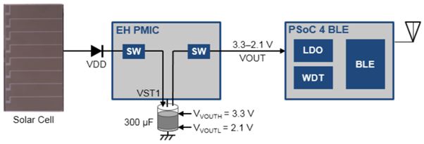
Figure 6: Simple energy harvesting design
First, the PMIC stores the solar energy in a storage device VSTORE1 (VST1), in this case a 300-μF ceramic capacitor. When VST 1 reaches VOUTH V, energy can be transmitted to the MCU. However, this simple energy harvesting design cannot operate on a full-day basis because there is no backup capacitor. Let's take a look at how a backup capacitor is added to the PMIC device and how the capacitor can support the MCU.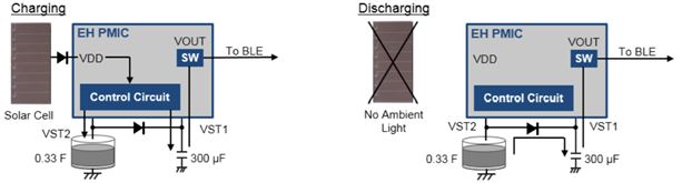
Figure 7: Energy Harvesting and Backup Capacitors
The energy required to operate the WSN is first stored in VST 1, and the remaining energy is used to charge VST 2. The energy stored in VST 2 can be continuously provided to WSN without light irradiation. In addition, an additional coin cell battery can be connected to the PMIC to increase reliability, as shown in Figure 8.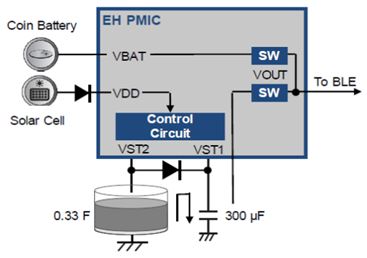
Figure 8: Energy collection from multiple power inputs
The PMIC converts both energy sources so that the WSN can operate under all conditions, even without lights. Conversions are automatically generated so that energy is supplied to WSN when needed. Therefore, this should be the most appropriate hardware design for WSN.Step 5: Designing the user interface <br> The user interface design connected to the wireless sensor node can be a mobile application that receives data from the WSN. Since the sensor's data may appear in a fixed position in the broadcast package, BLE applications can be designed to extract relevant data from these locations and display the data on your mobile phone. This technique can be used to manage a complex network of multiple WSNs.
ZGAR PCC KIT
ZGAR electronic cigarette uses high-tech R&D, food grade disposable pod device and high-quality raw material. All package designs are Original IP. Our designer team is from Hong Kong. We have very high requirements for product quality, flavors taste and packaging design. The E-liquid is imported, materials are food grade, and assembly plant is medical-grade dust-free workshops.
From production to packaging, the whole system of tracking, efficient and orderly process, achieving daily efficient output. We pay attention to the details of each process control. The first class dust-free production workshop has passed the GMP food and drug production standard certification, ensuring quality and safety. We choose the products with a traceability system, which can not only effectively track and trace all kinds of data, but also ensure good product quality.
We offer best price, high quality Vape Device, E-Cigarette Vape Pen, Disposable Device Vape,Vape Pen Atomizer, Electronic cigarette to all over the world.
Much Better Vaping Experience!


ZGAR PCC KIT E-Cigarette Vape Pen,ZGAR PCC KIT Disposable Device Vape,PCC SET,ZGAR PCC KIT Vape Pen Atomizer,ZGAR PCC KIT Disposable E-Cigarette OEM vape pen,ZGAR PCC KIT electronic cigarette
ZGAR INTERNATIONAL(HK)CO., LIMITED , https://www.zgarecigarette.com