In the design of FPGA-based digital systems, it is recommended to adopt a synchronous timing design, that is, a single clock system. However, in actual engineering, there are very few cases of pure single-clock system design, especially in the communication between design modules and peripheral chips, cross-clock domains are often inevitable. Improper handling of a series of problems such as metastability, sample loss, and potential logic errors caused by cross-clock domains will cause the system to fail to run. This article summarizes several synchronization strategies to solve the cross-clock domain problem.
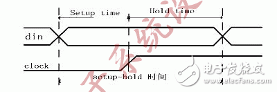
2 Metastability in asynchronous designFlip-flops are the most commonly used basic devices in FPGA design. There are setup and hold time of data in the trigger working process. For a flip-flop that uses a rising edge to trigger, the setup time is the minimum time for the data at the flip-flop to remain stable before the rising edge of the clock arrives. The hold time is the minimum time that the data at the flip-flop data terminal should continue to remain stable after the rising edge of the clock arrives. We call this time the setup-hold time (as shown in Figure 1). Within this time parameter, the input signal is not allowed to change on the rising edge of the clock. If the input signal changes during this time, the output result will be unknowable, that is, metastability.
When a signal transitions to another clock domain, if only a flip-flop is used to latch it, then the sampled result may be metastable. This is the problem that should be paid attention to when the signal crosses the clock domain. as shown in picture 2.
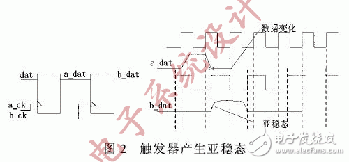
The output data of the signal dat through a latch is a_dat. When sampling with the clock b_clk, if a_dat happens to change within the setup-hold time of b_clk, then b_dat is neither a logic "1" nor a logic "0", but in an intermediate state. After a period of time, it may rise to a high level or decrease to a low level. The period from when the output signal is in the intermediate state to when it returns to logic "1" or logic "0" is called metastable time.
The time when the trigger enters the metastable state can be described by the parameter MTBF (Mean Time Between Failures). MTBF is the time interval for the trigger sampling failure, expressed as:

Among them, fclock represents the system clock frequency, fdata represents the frequency of the asynchronous input signal, tmet represents the longest metastable time that will not cause failure, and C1 and C2 are constants related to device characteristics. If the MTBF is large, it is considered that the design can operate normally in actual work and will not cause the failure of the entire system due to metastability. When the flip-flop is in a metastable state, and the time in the metastable state exceeds one clock cycle, this uncertain state will also affect the next level of flip-flops, and eventually lead to a chain reaction, thereby causing the entire system to malfunction.
3 Synchronization strategyIn asynchronous design, it is impossible to completely avoid metastability. Therefore, the basic idea of ​​the design should be: First, minimize the possibility of metastable state, and secondly, minimize the possibility of metastable state and bring harm to the system. The following are several synchronization strategies based on actual work.
3.1 Double latch methodIn order to avoid entering the metastable state, the parameter MTBF should be as large as possible. The commonly used method is the double latch method, that is, before a signal enters another clock domain, the signal is latched twice with two latches (as shown in Figure 3). Theoretical research shows that this design can reduce the probability of metastability to a very small extent, but this method also brings a first-level delay to the input signal, which needs to be paid attention to when designing the clock.
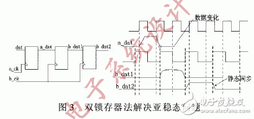
For the above double latch method, if the frequency of a_clk is higher than the frequency of b_clk, there may be a problem that b_clk cannot be sampled because dat changes too fast. That is, when the signal transitions from the fast clock domain to the slow clock domain, if the signal changes too fast, the slow clock may not be able to sample the signal correctly, so when using the double latch method, the original signal should be kept Long enough time so that the latch of another clock domain can sample it correctly.
3.2 Tie rope methodSince the double latch method may have the problem of sampling failure in the transition from the fast clock domain to the slow clock domain, we have introduced a safe cross-clock domain method: the rope method. The knot method is suitable for the transition of any clock domain (the frequency and phase relationship of clk1, clk2 can be arbitrarily selected), as shown in Figure 4.
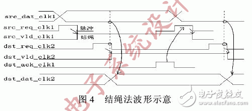
_Clk1 in Figure 4 indicates that the signal belongs to the clk1 clock domain, and the signal of _clk2 indicates that the signal belongs to the clk2 clock domain. The rope is tied by src_vld_clk1 (Pluse2Toggle) between two src_req_clk1. After synchronizing src_vld-clk1 with double latches, the signal is converted to dst_req_clk2 (Toggle2Pluse). In the same way, use dst_vld_clk2 to tie dat_req_clk2. dst_vld_clk2 indicates that in the clk2 clock domain, src_dat_clk1 can already be sampled correctly. Finally, convert dst_vld_clk2 to dst_ack_clk1 (Synchronizer and Toggle2Pluse). dst_ack_clk indicates that src_dat_clk1 has been correctly sampled by clk2, and then the clk1 clock domain can safely transmit the next data. It can be seen that the key of the knotting method is to keep the signal long enough after knotting the rope so that another clock can sample correctly. Figure 5 describes the specific implementation of the knot method, which mainly includes three basic units: Pluse2Toggle, Synchronizer and Toggle2Pluse.
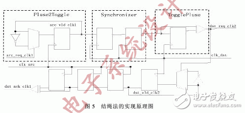
The Pluse2Toggle module is responsible for tying the two pulse signals, that is, extending the single pulse signal; the Synchronizer module uses the double latch method to transfer the obtained signal to another clock domain; the Toggle2Pluse module is opposite to the Pluse2Toggle function, which is to restore the extended pulse signal to For single pulse, an exclusive OR gate is used here. The overall design idea is to extend the signal with Pluse2Toggle, transition with Synchronizer, and restore with Toggle2Pluse to ensure that another clock domain can be sampled correctly, and the receiver uses the opposite process to send back the response signal.
The knotting method can solve the problem of transition from the fast clock domain to the slow clock domain, and has a wide range of applications. However, the knotting method is more complicated to implement and should be used with caution in occasions with higher design requirements.
4 ConclusionThis article mainly analyzes the problems that arise in the FPGA asynchronous clock design, the reasons and the synchronization strategies used to solve the problems in detail. Among them, the double latch method is more suitable for only a few signals across the clock domain; the knotting method is more suitable for the transition from the fast clock domain to the slow clock. Therefore, in actual applications, an appropriate synchronization strategy should be selected according to the characteristics of its own design.
Heating Element Temperature Control,Electric Grill Temperature Controller,Thermostat For Heating Element,Oven Capillary Thermostat
Foshan City Jiulong Machine Co., Ltd , https://www.jlthermostat.com