Switching power supply is a kind of power supply that uses modern power electronic technology to control the time ratio of switching on and off to maintain a stable output voltage. Switching power supplies are generally composed of pulse width modulation (PWM) control ICs and MOSFETs. With the development and innovation of power electronics technology, switching power supply technology is constantly innovating. At present, the switching power supply is widely used in almost all electronic equipment due to its small size, light weight and high efficiency. It is an indispensable power supply method for the rapid development of today's electronic information industry.
Basic circuit block diagram of switching power supplyAfter the AC voltage is rectified and filtered by the rectifier circuit and the filter circuit, it becomes a DC voltage with certain pulsating components. The voltage is converted into a square wave of the required voltage value by the high-frequency converter, and finally the square wave voltage is rectified The filtering becomes the required DC voltage.
The control circuit is a pulse width modulator, which is mainly composed of a sampler, a comparator, an oscillator, a pulse width modulation and a reference voltage circuit. This part of the circuit has been integrated, and various integrated circuits for switching power supplies have been made. The control circuit is used to adjust the ratio of the switching time of the high-frequency switching element to achieve the purpose of stabilizing the output voltage.
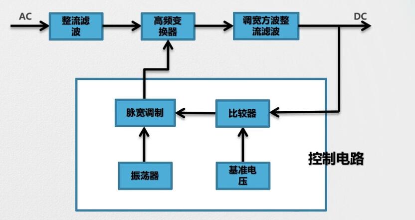
The basic principle of switching power supply is shown in the figure. It is mainly composed of the following 7 parts:
1) Input rectifier filter, including rectifier bridge and input filter capacitor;
2) Monolithic switching power supply, including power switch tube and controller (including oscillator, reference voltage source, error amplifier and PWM comparator), MOSFET;
3) Drain clamp protection circuit;
4) High frequency transformer;
5) Output rectifier filter;
6) Optocoupler feedback circuit;
7) Bias circuit, which provides bias voltage to the photosensitive of the optocoupler.
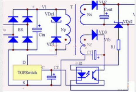
The principle of voltage stabilization is analyzed as follows:
When V rises due to some reason, the current on the LED increases, and the emitter current of the receiving tube rises through the optocoupler, which in turn makes the control terminal current of TOPSWITCH larger and the duty cycle smaller, causing V to drop. , So as to achieve the effect of voltage stabilization.
Switching power supply circuit diagram explanation (1)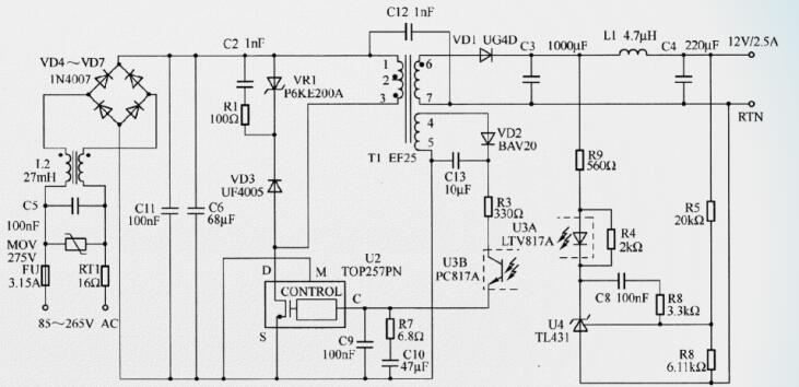
The picture shows a 30W, 12V output switching power supply circuit diagram. The power supply circuit has the characteristics of low cost, small number of components, small and light, high energy efficiency, low no-load and standby power consumption, etc., the no-load power consumption is less than 250mW when 265V AC input, and the output when working under 50°C The power is 30W, no external heat sink is needed, and it has a precise auto-recovery and hysteresis characteristic overheating shutdown function, which keeps the PCB temperature within a safe range under various conditions, when the output is short-circuited and the feedback loop is open. It enters the automatic restart protection state, and has excellent input voltage regulation and load regulation. It meets the requirements of EN55022 and CISPR-22B for EMI limits, and the EMI margin is greater than 10dBuV.
Switching power supply circuit diagram explanation (two)12v switching power supply circuit diagram
The schematic diagram of the 12v switching power supply is explained. The switching power supply is a low-power switching power supply, input 220V AC mains, output 12V DC, maximum output current 1.3A, mainly used in the power supply of small equipment, such as building monitoring equipment. The electrical schematic diagram is shown in Figure 1. Its control core device is pulse width modulation integrated circuit TL3843P (contains oscillator, pulse width modulation comparator, logic controller, with over-current, under-voltage protection and control functions, the highest operating frequency can reach 500MHz. Starting current only needs ImA ). The functions of each pin are as follows: (1) pin is the output end of the internal error amplifier, usually there is a feedback network with (2) pin to determine the gain of the error amplifier. (2) The pin is the feedback voltage input terminal, as the inverting input terminal of the internal error amplifier, compared with the reference voltage (+2.5V) of the non-inverting input terminal to generate the error control voltage and control the pulse width. (6) At the pin overcurrent detection input terminal, when the voltage connected to the person is higher than 1V, the output of the drive pulse is prohibited. (4) The pin is the common connection terminal of RT/RC timing resistor and capacitor, used to generate sawtooth oscillation wave. (5) The foot is the ground terminal. (6) The pin is the pulse output terminal with adjustable pulse width. (7) The pin is the working voltage input terminal (10V》Vi≤30V). (8) The pin is the output terminal of the internal reference voltage (VREF=5v).
Switching power supply circuit diagram explanation (3)24 Switching power supply circuit diagram
The circuit takes the UC3842 oscillator chip as the core to form an inverter and rectifier circuit. UC3842 is a high-performance single-ended output current-controlled pulse-width modulator chip. The related pin functions and internal circuit principles have been introduced, so they are omitted here. The AC220V power supply is introduced through the common mode filter L1, which can better suppress the high frequency interference from the power grid and the radiation from the power supply itself. The AC voltage is filtered by the bridge rectifier circuit and the capacitor C4 to become an unstable DC voltage of about 280V. An inverter circuit composed of an oscillating chip U1, a switching tube Q1, a switching transformer T1 and other components. The inverter circuit can be divided into four circuit parts to explain the working principle of the circuit.
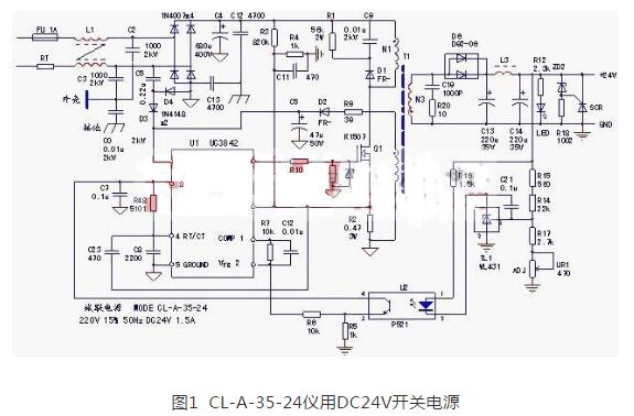
1. Oscillation circuit: the drain-source of the main winding N1 and Q1 of the switching transformer, R2 (working current detection resistance) is the path of the power supply working current; the starting circuit of this machine and other switching power supplies (the starting circuit is limited by the step-down current The resistance composition) is different. The starting circuit is composed of C5, D3, and D4, which provide a "transient" starting current. The diode D2 absorbs the reverse voltage, and D3 has a rectifier function to ensure that the starting current added to the 7th pin of U1 is Positive current: After the circuit starts to oscillate, the N2 self-powered winding, D2 and C5 rectifier filter circuit provide the power supply voltage of the U1 chip. The normal operation of these three links is a prerequisite for the power supply to oscillate.
Of course, U1's 4-pin external timing components R48, C8 and U1 chip itself also constitute a part of the oscillation circuit.
Capacitive start circuit, when overload or short circuit fault occurs, the circuit can be in a stable vibration stop protection state, unlike the resistance start circuit, it will reproduce the "hiccup" intermittent oscillation phenomenon. The working current detection is obtained from the resistor R2. When the fault condition causes an abnormal increase in the working overcurrent, the duty cycle of the PWM pulse output at pin 6 of U1 will decrease, and the induction circuit of the self-powered winding of N1 will also decrease. When the pin supply voltage is lower than 10V, the circuit stops vibrating and the load voltage is 0. This is the output suspension caused by the action of the U1 internal undervoltage protection circuit caused by overcurrent (overload or short circuit); when the working current increases abnormally, the voltage on R2 When the drop is greater than 1V, the internal latch will act and the circuit will stop oscillating. This is caused by the over-current caused by the U1 internal over-current protection action and the output is suspended.
2. Voltage stabilization circuit: 24V power supply composed of N3 winding, D6, C13, C14 and other components of the switching transformer, reference voltage source TL1, optocoupler U2 and other components constitute a voltage stabilization control circuit. The U1 chip and the peripheral components R7 and C12 on pins 1 and 2 are also part of the voltage regulator loop. In fact, TL1 and U1 constitute (relative to the internal voltage error amplifier of U1) an external error amplifier, which feeds back the voltage change of the output 24V to the feedback voltage signal input terminal of U1. When the 24V output voltage rises, the voltage of pin 2 of U1 rises, the voltage of pin 1 drops, the duty cycle of the output PWM pulse drops, and the output circuit drops. When the output voltage rises abnormally, when pin 1 of U1 drops to 1V, the internal protection circuit operates and the circuit stops oscillating.
3. Protection circuit: The U1 chip itself and the 3-pin peripheral circuit constitute an overcurrent protection circuit; the D1, R1, and C9 components connected in parallel on the N1 winding constitute the reverse voltage absorption protection circuit of the switch tube to provide the reverse when Q1 is off The current path ensures the safety of Q1's work; in fact, the voltage feedback signal of the voltage regulator loop can also be regarded as a voltage protection signal-when the feedback voltage amplitude reaches a certain value, the circuit will implement the vibration stop protection action; 24V output An overvoltage protection circuit composed of R18, ZD2, and unidirectional thyristor SCR is connected in parallel. When the voltage stabilizing circuit malfunctions and causes an abnormal rise in the output voltage, the breakdown of the Zener diode ZD2 provides the trigger current for the SCR, and the conduction of the SCR forms a The "short-circuit current" signal forces the U1 internal protection circuit to produce an overcurrent protection action, and the circuit is in a state of vibration stop.
2D Barcode Scanner
Features
Material:TPU+PC, more rugged than ABS + PC, more stronger fall resistance
Charging Base:charging base not only charge ring scanner but also can be regarded as a bluetooth adapter to connect ring scanner with PC
Compatible With Most Operation System:We can provide the software(Bluetooth input method)for Windows and Android, By the way, there are corresponding SDK
Applicable scope
1.Comercial POS system(Supermarkets
2.Warehousing and logistics
3.Libraries
4.Banks and Telecom
5.Transportaion
6.Postal service
7.Industrial and manufacturing management
2D Barcode Scanner,Data Matrix Barcode Scanner,2D Barcode Scanner Usb,1D 2D Scanner
ShengXiaoBang(GZ) Material Union Technology Co.Ltd , http://www.sxbgz.com