A member of SWIFTTM's family of DC/DC regulators, the TPS5430 is a high output current PWM converter that integrates a low impedance, high side N-channel MOSFET. It integrates a high-performance voltage error amplifier with tight voltage regulation accuracy under transient conditions, an undervoltage lockout function to prevent the input voltage from starting at 5,5V, and a built-in slow-start circuit to limit inrush current. The voltage feedforward circuit improves transient response. Other features include a sensitive high level enable, over current protection and thermal shutdown. To reduce the complexity of the design and the number of external components, the TPS5430 has an internal feedback compensation loop.
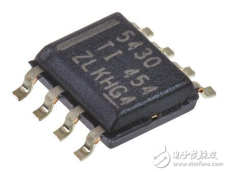
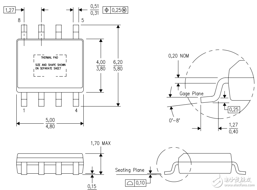
The TPS5430 device is thermally enhanced for easy access in an 8-pin soic powerpadmm package. TI offers evaluation modules and software tools from SWIFTTM designers to help design high-performance power supplies as quickly as possible to meet shorter development cycles.
These devices have limited built-in ESD protection. The leads should be shorted together or placed in a conductive foam placed in the reservoir to prevent static damage to the MOS gate.
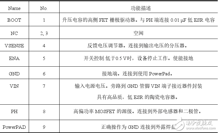
Tps5430 pin diagram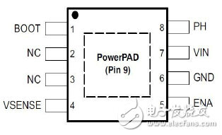
The specific instructions are as follows:
1 undervoltage lockout (UVLO)
When VIN (input voltage) is below the UVLO startup voltage threshold, the TPS5430 uses an undervoltage lockout circuit to keep the device disabled. At power-up, the internal circuit operates inactive until the input voltage exceeds the UVLO threshold voltage. Once the undervoltage lockout threshold voltage reaches the startup voltage, the device begins to start. The device operates until the input voltage drops below the UVLO threshold voltage. The typical hysteresis voltage in the UVLO comparator is 330mV.
2 boost capacitor
Connect a 0.01uF low ESR Ceramic Capacitor between the PH pin and the BOOT pin. This capacitor provides the high side MOSFET gate drive voltage.
3 output feedback (VSENSE) and internal compensation
The regulator output voltage is set by the external resistor divider from the feedback to the VSENSE pin. During steady state operation, the VSENSE pin voltage should be equal to the reference voltage of 1.221V. The TPS5430 implements internal compensation to simplify the design of the Zener. Because the TPS5430 uses voltage mode control, in order to provide high crossover frequency and high stability phase margin, the chip design uses a type III compensation network.
4 voltage feedforward
The internal voltage feedforward provides a constant DC power stage gain despite variations in the input voltage. This greatly simplifies the stability analysis and improves the transient response. The feedforward voltage is inversely proportional to the peak ramp voltage of the input voltage, so that the modulator and power stage gains are constant with feedback gain, and the TPS5430 typically has a feedforward gain of 25.
5 pulse width modulation (PWM) control
The regulator uses a fixed frequency pulse width modulation (PWM) control method. First, the feedback voltage (VSENSE pin voltage) is compared to the reference constant voltage using a high gain error amplifier and a compensation network to generate an error voltage. The error voltage is then compared to the ramp voltage by a PWM comparator. Thus, the error voltage amplitude is converted into a pulse width, that is, a duty ratio. Finally, the output of the PWM is fed back to the gate drive circuit to control the turn-on time and frequency of the upper high-side MOSFET.
6 overcurrent protection
Overcurrent protection operates by detecting the drain-to-source voltage of the high-side MOSFET. The drain-source voltage is then compared to a threshold voltage value representative of an overcurrent threshold. If the drain-source voltage exceeds the overcurrent threshold threshold, the overcurrent flag is set to true. The system will ignore the overcurrent indication of the leading edge blanking time at the beginning of each cycle to avoid any noise failure.
Once the overcurrent flag is set to true, overcurrent protection is triggered. The high-side MOSFET will turn off after a certain delay, ready for the next cycle. Overcurrent protection is the so-called cycle current limit. If the sense current continues to increase during the cycle-by-cycle current limit period, the "intermittent" mode of the overcurrent protection is triggered to replace the cycle-by-cycle current limit mode. In the "intermittent" mode overcurrent protection, the reference voltage is grounded and the high-side MOSFET is turned off, ready for the next "intermittent". Once the "intermittent" duration is complete, the regulator is restarted under the control of the slow start circuit.
Reverse Conducting Thyristor(RCT)
Reverse Conducting Thyristor(RCT) is also called Reverse- appreciation Thyristor.The characteristic is that a diode is connected in reverse parallel between the anode and cathode of thyristor, so that the transmitting junction of anode and cathode is short-circuited.As a result of this special circuit structure, it has high voltage resistance, high temperature resistance, short turn-off time, low switching voltage and other good performance.For example, the turn-off time of the reverse thyristor is only a few microseconds, and the working frequency is dozens of KHZ, which is better than the fast thyristor (FSCR).This device is suitable for switching power supply and UPS uninterrupted power supply. One RCT can replace one thyristor and one continuous current diode respectively.
Reverse Conducting Thyristor,Original Reverse Conducting Thyristor,New Reverse Conducting Thyristor,Reverse-Conducting Thyristor 2200V
YANGZHOU POSITIONING TECH CO., LTD. , https://www.pst-thyristor.com