The Global Navigation Satellite System (GNSS) is an important infrastructure for maintaining national security and developing the economy, and an important symbol of the country's comprehensive national strength and the international influence of a modern power. The development of receiver terminals supporting the Beidou navigation system is an indispensable part of the Beidou navigation system. At present, China is vigorously developing the Beidou satellite navigation system (BDS). Therefore, vigorous research and design of the Beidou satellite navigation receiver based on BDS has become an important part of the Beidou satellite navigation system.
Semiconductor integration is developing rapidly, and it is currently developing towards converging silicon wafers. FPGA is no exception in this direction. General-purpose processors, IP with ASSP and DSP functions are continuously integrated into FPGA; the continuous innovation and breakthrough of FPGA technology, and the introduction of silicon converged architecture products, will inevitably make FPGA applications Many areas that have not been involved before. With the advancement of technology, the development of SoC highly integrated single-chip receivers will become the main direction of future satellite navigation receiver development.
1 SoC hardware system designThe system uses Intel 28 nm process low-power Cyclone V 5CSEM5F31C6N SoC FPGA as the main control chip. The hardware system design of the carrier tracking loop based on SoC FPGA is shown in Figure 1.
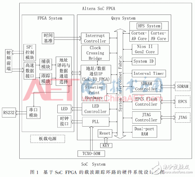
The SoC System is mainly composed of two parts, including the hardware design of the Qsys System (embedded system) part and the FPGA System (FPGA logic unit system) hardware design based on Verilog HDL.
1.1 Qsys System design
According to the design in Figure 1, the Qsys system is built using Qsys tools, and the interconnection is shown in Figure 2.
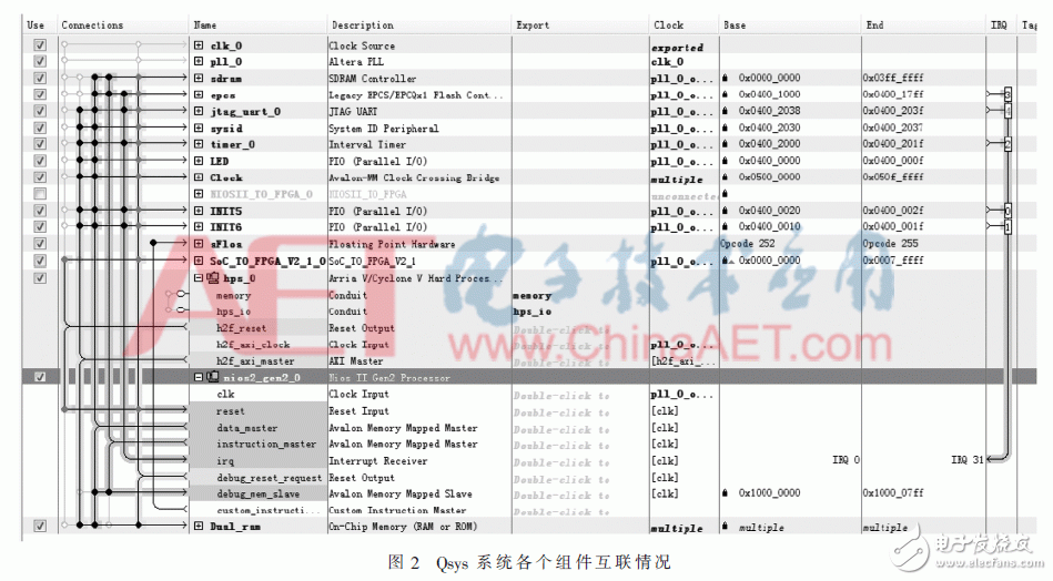
The function design of each part of the system is as follows:
(1) clk_0 is an external clock and reset input, which provides TCXO-50M clock input and system reset signal for PLL.
(2) pll_0 is the PLL in Figure 1, which provides 6 clocks, outclk0 and outclk5 are provided to each component in Qsys; outclk1 provides clocks for off-chip SDRAM; the remaining 3 clocks are output externally for each module in the FPGA System Drive clock.
(3) sdram is the SDRAM Controller in Figure 1, used to control the off-chip SDRAM chip, which serves as the memory of Nios II Gen2 Core.
(4) epcs is the EPCS Flash Controller in Figure 1, which controls external Flash and serves as the program memory of Nios II Gen2 Core.
(5) jtag_uart_0 is the JTAG Controller in Figure 1, which is connected to the debug port of Eclipse SBT on the PC host for program monitoring and debugging.
(6) sysid is the System ID in Figure 1, to ensure that the software program version is consistent with the Qsys system version.
(7) TImer_0 is the Interval TImer in Figure 1, which can be used for the Nios II Gen2 Core core clock, and can also be used to test the running time of the program. The corresponding test and debugging can be performed according to the measured time.
(8) LED is the LED Controller in Figure 1, where the PIO core is designed as an output function, and the bit width of the output data is set to 6 bits to control the 6 LEDs of the FPGA System to test and prompt the running status of the system.
(9) Clock is the Avalon-MM Clock Crossing Bridge in Figure 1, used to connect to the Avalon bus and belong to data transmission and communication between IP cores in different clock domains.
(10) INIT5 and INIT6 are the Interrupt Controllers in Figure 1, where the PIO core is set to interrupt signal input function, the bit width of INIT5 and INIT6 is designed to be 1 bit, and the interrupt mode is set to edge (rising edge) trigger. INIT5 and INIT6 are respectively used to receive 2 interrupt signals generated by FPGASystem.
(11) aFloa is the Floatin Point Hardware in Figure 1, which is used to accelerate the floating-point computing hardware of Nios II Gen2 Core.
(12) SoC_TO_FPGA_V2_1_0 is the address data communication IP in Figure 1. This interface is used for two-way data transmission between FPGA System and Qsys System.
(13) hps_0 is the HPS System in Figure 1, and hps_0 is the main CPU of the post-positioning solution and graphical interface. Due to the requirement to support the Linux system, some peripherals need to be set up, including peripherals such as EMAC, QSPI, SD/MMC, USBOTG, SPI, UART, I2C, and some GPIOs.
(14) nios2_gen2_0 is the Nios II Gen2 Core in Figure 1, designed as the main CPU of the baseband signal processing system.
(15) Dual_ram The Dual-port RAM shown in Figure 1 provides data communication between HPS and Nios II Gen2 Core; the relationship block diagram between HPS, Nios II Gen2 Core and Dual-port RAM is shown in Figure 3.
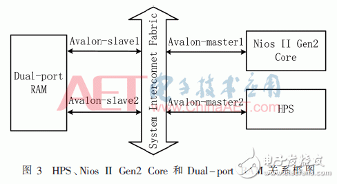
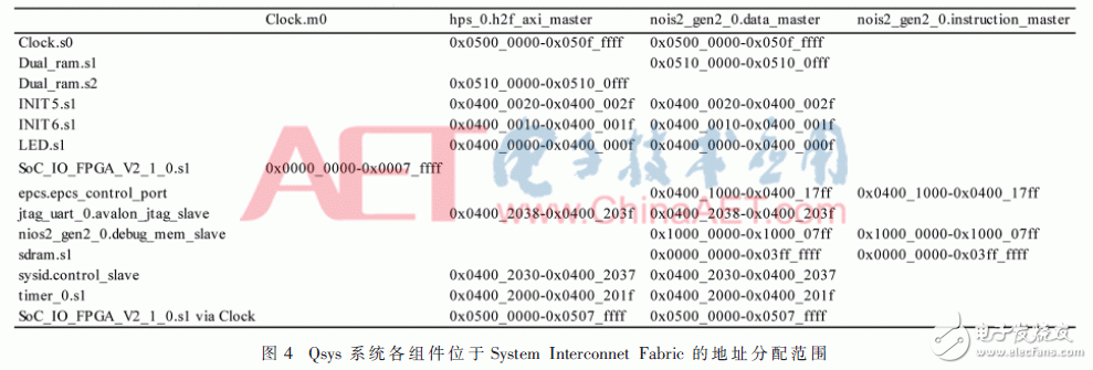
Figure 4 shows the address allocation of each component of the Qsys system in the System Interconnet Fabric.
1.2 FPGA System design
FPGA System is mainly composed of SPI control module, high-speed data interface, time reference module, capture module, tracking module, serial port module, address decoding and data channel selection module. The functions of each part are as follows:
(1) The SPI control module is used to control the radio frequency board to generate a 1 550 MHz local oscillator carrier signal, which is mixed with the antenna received signal to generate 3.098 MHz intermediate frequency data.
(2) The high-speed data interface is used to obtain the high-speed ADC quantization of the radio frequency front-end to generate I/Q two-channel 8 bit data, and each channel intercepts the high 4 bit data for baseband processing.
(3) The time reference module is used to generate 2 interrupt signals, including 0.5 ms and 20 ms interrupts.
(4) The capture module is used for satellite capture, and the capture channel is a single channel design.
(5) The tracking module is used for satellite tracking. The number of tracking channels is currently designed to be 24 channels.
(6) The serial port module is used to output debugging information and navigation messages.
(7) The address decoding and data channel selection module is used to decode the address and select different data channels according to the address information.
2 Carrier loop design2.1 Carrier ring discriminator
Since the satellite signal is modulated with navigation messages, the received intermediate frequency signal will produce a 180° phase jump when the data bit level jumps. Therefore, in order to maintain the stability of the loop, the 180° phase jump must be eliminated change. Since the phase detector invented by COSTAS JP can not be affected by data bits, the phase detector he invented is called Costas phase detector (or Costas phase detector), and the phase lock using these phase detectors The ring is called the Costas ring (or Costas ring).
The phase-locked loop discriminator of this design adopts the classic Costas loop phase discriminator Qp×Ip, which has approximately optimized phase discrimination properties when the signal-to-noise ratio is low, the output result is proportional to the square of the amplitude, and the amount of calculation It is small and the phase discrimination slope is greatly affected by the signal amplitude.
In this paper, the frequency-locked loop discriminator is designed using cross product discriminator Pcross/(t2-t1), which has a near-optimized frequency discrimination characteristic in the case of low signal-to-noise ratio, the slope is proportional to the square of the signal amplitude, and the amount of calculation is minimal. Affected by signal amplitude.
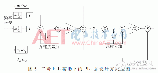
2.2 Loop filter
The design idea of ​​the software program is to place the processing program of the tracking loop in the 0.5 ms interrupt. The 0.5 ms interrupt queries each channel in turn, and selects whether to perform traction or tracking according to the current tracking channel state: if it is in the traction state, the traction subroutine will be called ; If it is in tracking state, the tracking subroutine will be called. Its running process is shown in Figure 6.
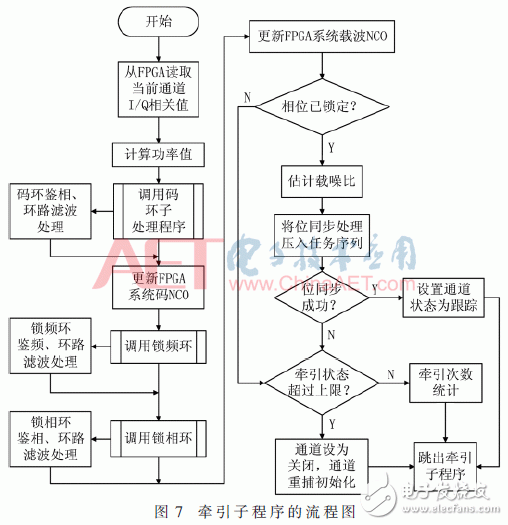
The traction subroutine includes reading the I/Q related amplitude from the FPGA, and after calculating the power, calling the code loop, frequency locked loop, and phase locked loop processing subroutines respectively. The code loop, frequency locked loop, and phase locked loop are subjected to frequency discrimination and discrimination. After phase and loop filtering, update the code NCO and carrier NCO inside the FPGA, and set the current channel state according to the bit synchronization: if the synchronization is successful, set the current channel to the tracking state; if the synchronization is unsuccessful, the number of pulls will be performed Statistics, if the statistics threshold is exceeded, the channel is set to close, the channel is recaptured and initialized, and then jump out of the traction subroutine, otherwise directly jump out of the traction subroutine. The traction processing subroutine is shown in Figure 7.
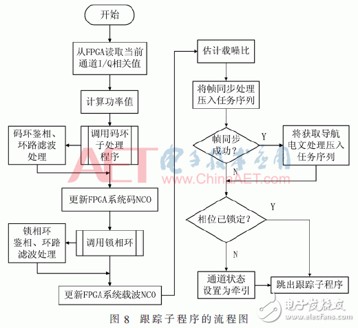
The tracking subroutine includes reading I/Q related amplitudes from FPGA, calling code loop and phase-locked loop processing subroutines after calculating the power, and updating the internal FPGA after the code loop and phase-locked loop are processed by phase detection and loop filtering. Set the task status according to the frame synchronization status: if the synchronization is successful, push the navigation message processing task into the task queue; determine the phase lock status, if the phase lock fails, set the channel status to traction Status, and then jump out of the tracking subroutine. The tracking processing subroutine is shown in Figure 8.
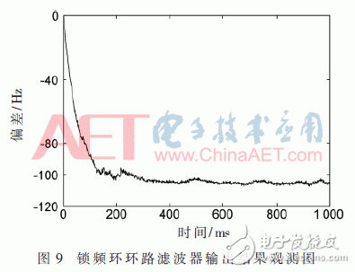
After the signal enters the traction, use Nios II SBT for Eclipse to collect the output value of the frequency-locked loop filter, and use MATLAB to simulate the change of the output value of the frequency-locked loop filter with time, as shown in Figure 9. It can be seen from the figure that at time 0, the absolute value of the frequency error is about 100 Hz; in the interval of 0 to 300 ms, the absolute value of the instantaneous frequency error output by the loop gradually decreases with time; at the time of 300 ms, the loop The absolute value of the output instantaneous frequency error is close to 0, and then the phase-locked loop takes over to further process the phase error.
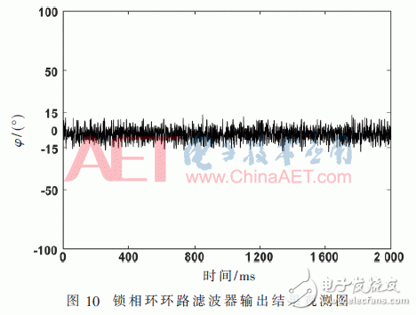
Use Nios II SBT for Eclipse to collect the output value of the phase-locked loop loop filter, and use MATLAB to simulate the change of the output value of the phase-locked loop loop filter with time, as shown in Figure 10. According to the design of the tracking subroutine in Section 3, the precision tracking stage passes through the traction stage to eliminate the influence of the frequency error and then uses the phase-locked loop for precision tracking. It can be seen from the figure that the phase error range of the phase-locked loop basically fluctuates within ±15°.
According to the requirements of baseband signal processing, this paper uses SoC FPGA as the design platform, completed the design of Beidou satellite signal tracking algorithm on a single chip, and tested and verified the corresponding carrier loop algorithm. The results show that the tracking algorithm fully meets the real-time requirements of the Beidou satellite navigation receiver.
DC meter for solar power multi-channel monitoring. This is a multi-channel power measuring system with LCD display and Modbus RTU communication, available 9 DC channels or 21 channels with an external module provides current, voltage, frequency and bi-directional energy electricity parameters. It`s a perfect measuring component for the renewable power generation industry such as wind power, PV solar power etc.
Dc Multi-Channels Power Meter,Ev Charger Digital Power Meter,Ev Charger Dc Power Meter Multifunctional,Multi-Channel Power Meter For Solar
Jiangsu Sfere Electric Co., Ltd , https://www.elecnova-global.com