The causes of EMC radiation exceeding the standard are various. The interface filtering is not good, the structure screen effect is low, and the cable design is defective. The radiation emission may exceed the standard, but the root cause of the radiation is in the PCB design. Focus on PCB from EMC, mainly focusing on these aspects:
(1) From the perspective of reducing radiation disturbance, the multi-layer board should be selected as much as possible. The inner layer is used as the power layer and the ground layer respectively to reduce the impedance of the power supply line, suppress the common impedance noise, and form a uniform ground plane for the signal line. The distributed capacitance between the large signal line and the ground plane suppresses its ability to radiate into space.
(2) The power line, ground line, and printed board trace should maintain low impedance to high frequency signals. At very high frequencies, power lines, ground lines, or printed circuit board traces can become small antennas for receiving and transmitting disturbances. In addition to adding filter capacitors, the method of reducing such disturbances is more important to reduce the high-frequency impedance of the power lines, ground lines, and other printed circuit board traces. Therefore, the traces of various printed boards should be short and thick, and the lines should be even.
(3) The power cable, ground wire and printed conductor should be arranged on the printed board properly, so as to be short and straight as possible to reduce the loop area formed between the signal line and the return line.
(4) The layout of circuit components and signal paths must minimize the mutual coupling of unwanted signals.
The issues of concern at different stages of the PCB are different.
At the component layout stage, you need to pay attention to:
1. Whether the device for filtering, protecting and isolating the interface signal is placed close to the interface connector, first protection, and then filtering; whether the power module, filter, and power protection device are placed near the entrance of the power supply, and the input line of the power supply is kept as short as possible. The input and output of the power supply are separated, and the traces do not cross each other;
2. Whether the strong radiation device or sensitive device such as crystal, crystal oscillator, relay, switching power supply, etc. is far away from the single-handle handle bar and connector;
3. Whether the filter capacitor is placed close to the power pin of the IC, and the position and quantity are appropriate;
4. Whether the clock circuit is close to the load and the load is balanced;
5. Whether the input and output of the interface filter component do not cross the partition; except for optocouplers, magnetic beads, isolation transformers, A/D, D/A, etc., whether other devices do not cross the partition;
Pay attention to the PCB layout stage:
1. The wiring of the power supply and the ground is processed without a ground loop, and the power supply and the corresponding loop area are small;
2. Whether the differential signal line pairs are in the same layer, equal length, and walking line, keep the impedance consistent, and there are no other traces between the differential lines;
3. Whether the key signal lines such as clocks are laid in the inner layer (prioritizing the preferred wiring layer), and adding shielded ground lines or other wiring spacing to meet the 3W principle, whether the key signal traces do not cross the partition;
4. Is there no other signal line to be routed from the input line of the power filter, and whether the input and output signal lines of the filter and other devices are not parallel to each other and cross-tracked;
Although we have developed a variety of PCB layout rules, when implementing these rules, no matter how hard we try, the defects in the design are always lingering like a disease. Because there are always reasons for this or that, because of the actual design, we can not fully meet the design rules. But often these places that cannot meet the rules will cause trouble for future certifications:
1.1 The radiation source is too close to the interface
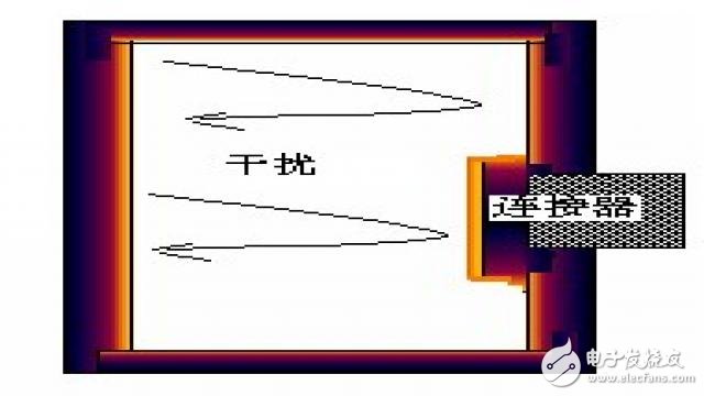
The most typical radiation source is the crystal oscillator. Every PCB engineer knows that the crystal oscillator should be far away from the I/O interface. However, the PCB required by the product design engineer is often limited in size and has a large number of devices. Therefore, after various considerations, the PCB engineer “has to have "Place the crystal at the I/O interface." No matter how much you think about EMC in other places, an unreasonable crystal oscillator can easily destroy your efforts.
In the PCB design, first consider the discharge position of the radiation source, as far as possible away from the handle bar and the power input port. For the crystal oscillator, the shadow area on the PCB must be copper-plated, and the output lead wire is not allowed to go to the surface layer of the PCB, and should be taken in the inner layer (if it can be processed again, it is more ideal). In addition, PCB layer division and stratification are also a key factor affecting the radiation emission index, and should be considered in combination with the specific conditions of the board.
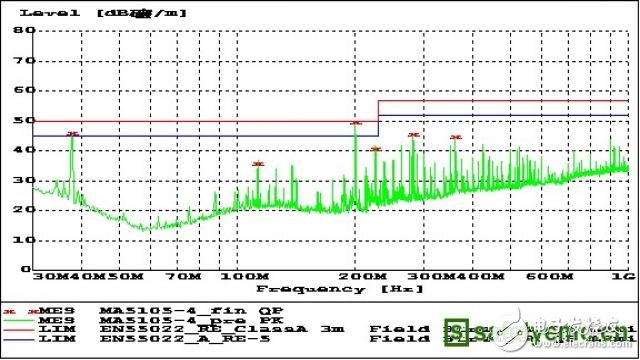
Classic case descriptionThe M product was tested by EMC. It was found that the frequency at 50MHz and 75MHz was severely exceeded. The amplitude of the 25MHz multiplier point at 100MHz, 125MHz, etc. was also very large, close to the CLASS A limit line.
From the experimental phenomenon that the higher frequency points are 25MHz multiplier, it is suspected that there is a 25MHz crystal oscillator inside the device and the crystal oscillator is improperly processed. After investigation, it was found that there are two kinds of interface boards with a 25MHz crystal oscillator. Near-field detection confirmed that the 25MHz multiplier point emission near the two boards was larger. Check the PCB of the board and find that the PCB and the processing of the crystal oscillator mainly have the following defects:
1. The crystal oscillator is too close to the handle bar;
2. The lead of the crystal output end goes a long distance on the surface of the PCB;
3. There is no complete copper plating in the shadow area of ​​the crystal on the PCB;
4. The crystal oscillator is too close to the power input port;
5, PCB layering is unreasonable, and only one layer of a 6-layer board is a layer that has been divided into many layers.
These factors provide a means of propagation for disturbances on the crystal. Harassment can be coupled to other boards and cables through adjacent traces and power lines, and can also be directly coupled outside the enclosure through space, causing excessive emissions.
After partial shielding and grounding treatment with copper foil on the outer shell of the crystal oscillator, the 25MHz harmonic between 100MHz and 300MHz is basically eliminated, and the amplitude of the 50MHz and 75MHZ frequency points is also greatly reduced by nearly 10dB, which can reach the target. Request, test passed.
1.2 key signal lines are not covered inside
The key signal line, especially the clock line, is also a basic common sense of PCB layout. But which lines are key signal lines? People often pay attention to the clock lines coming out of crystals, crystal oscillators, and clock drivers, but they often overlook another type of trace with periodic nature—such as a specific address line.
For the periodic signal line, it is not only necessary to avoid excessive routing on the surface layer, but also to consider whether to allow the inner layer to pass through the via hole for the trace adjacent to it in parallel.
Classic case descriptionWhen a product is tested at RE, there is a large amount of radiation at 37.5M. The test curve is as follows:
Because 37.5M is 3 times the frequency of 12.5M, we suspect that it is related to the 25M crystal on the board, so the output of the 33ohm resistor is disconnected. As a result, the 37.5M radiation is gone, and the nearby frequency band is also very clean. This shows that the 37.5M frequency is indeed related to the 25M clock.
After analysis, we found that the 37M clock flow graph is
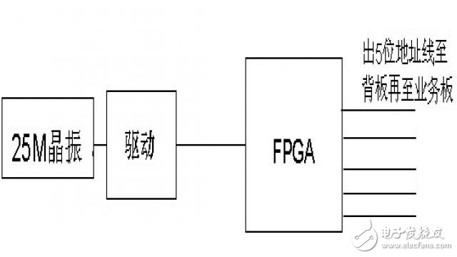
The A0, A1, A2, A3, and A4 address lines from the FPGA, in the no-service state, will generate the rule 01010101 according to the protocol requirements A3/A4. . . . . . The alternate signal, triggered by the rising edge of the 25M clock, has a frequency of 12.5MHz. 37.5MHZ is exactly its 3rd harmonic. The protocol requires that A0 A1 A2 level be added to 1F every time it changes, and its signal is not a square wave that changes periodically. Since we generally think that the interference of the address line is small and there is no periodic interference, we pay no attention to the PCB layout and routing, and walk on the surface layer, and the trace is very long, reaching the backplane and extending to other boards. The signals in the actual two address lines are periodic rectangular waves, which are exactly the same as the clock signal waveform. Longer traces, periodically changing signals, and surface traces cause the radiation of this section to exceed the standard. During the test, we cut off the matching resistance at the beginning of the two address lines of A3 A4, and the 37.5M interference disappeared, which proves that our judgment is correct.
After correcting the design flaws in subsequent revisions, 37.5M interference no longer occurs.
Unreasonable ground plane divisionAt the time of testing, the problem of splitting the power ground is also one of the most prone to problems. The problem of ground plane segmentation of power supply is an old problem in PCB EMC design. Different engineers have different opinions, and even have not reached a consensus. There are currently two opinions:
Viewpoint 1: Isolated Signal Ground System
The GND of the board is a separate system. It does not communicate with PGND. It forms a closed-loop system with the inside of the device and is connected to the outside only through DC/DC. The PGND on the board is an extension of the structure on the backplane and the board, which is used for shielding and shielding the energy release and anti-static of the device. BGND is a -48 return line. For safety reasons, BGND should be connected to the structure housing. Single point connection can be used. Usually, the power supply unit is connected to the equipment inlet, or the equipment power supply cabinet is shorted to BGND and PGND.
GND as the return ground of the digital signal, mainly the energy transfer relationship with the low-voltage power supply, its absolute potential does not affect the working state, it is important to generate a stable potential difference with the power supply to the device. Therefore, the reason for worrying about the interference level on the GND or the fact that the absolute potential is inconsistent with the casing is not sufficient. At this stage in the industry, the purpose of connecting GND to the chassis is to suppress high frequency noise on GND.
GND and the corresponding power supply act as an isolated system and do not create static build-up problems. Electrostatic accumulation is a prerequisite. First, there must be mutual friction between substances. Secondly, this friction can cause a large amount of charge transfer. Third, non-metals that can cause static accumulation of materials are often insulated, because these substances cannot In the slow discharge process with air, metals and other conductive materials have the characteristic of slowly discharging to the air, so they are less prone to static buildup. As long as the GND is completely isolated from the outside, it is not necessary to connect the GND resistor to the structure to discharge the electrostatic charge.
Viewpoint 2: Unified Signal System
The GND and structure of the product are completely merged into the same network. PGND represents the derived network of structures and structures on the back (single) board. PGND is GND on the electrical network. The key to this program is how to "unify"! The connection between GND and the structure is only "multi-point grounding" to meet EMC requirements. Therefore, each single board needs to be matched with a large metal plate, and the screws are connected to ensure good grounding, and the spacing between the grounding points satisfies the one-twentieth wavelength rule.
When GND is used as the signal return channel, it is GND. When used as static discharge, shielding, etc., it is PGND. The theoretical basis of this "one place and two use" is the theory of high frequency circuits and electromagnetic fields and electromagnetic waves. For any signal, the signal flows back to the lowest impedance path, not the physical minimum path. At high frequencies, the skin effect is significant. Even with a metal plate, the front and back facing high frequencies are two channels. The principle of minimum impedance and skin effect ensure that even if GND is connected to the structure, high-speed signal reflow will not be everywhere. It is always below the signal line, coupled with the signal line, and the loop inductance is minimized. This approach came into being with the increasing frequency of electronic products and the increasingly severe electromagnetic compatibility requirements. The difficulty in implementing this plan is that this scheme considers high frequencies but is risky for low frequency interference. Since the structure is actually connected to GND, the structure must be well connected to the ground. Otherwise, it will not vent the interference, but will also lead to interference and damage to the device. The second difficulty in achieving this solution is "grounding." If the GND of the board is connected by a single point and structure, this is not the "grounding" of the EMC. The consequence of this is that the high-frequency interference is still not contained, but the low-frequency interference is given to a channel. The EMC grounding must connect GND to the structure at multiple points, and the grounding distance between the grounding points should satisfy one-twentieth of the wavelength of the highest operating frequency of the device. Thirdly, the screw cannot be completely grounded. The veneer must be a metallized hole. The copper is directly in contact with the plane “face-to-face†of the structure plane, and the screw can be used. Because the screw is not grounded, the screw cannot reach the screw. High frequency grounding requirements. The implementation of these measures is to achieve the purpose of "GND grounding", otherwise it is only a form of grounding, in fact, "bad grounding."
The advantage of this scheme is that the interference on the GND is discharged to the earth through the structural low-impedance channel, which reduces the spatial radiation amplitude and is beneficial to the EMC. The disadvantage is that the complexity of the grounding system is increased and the structural cost is increased.
BGND is a -48 return line. For the same reason, BGND should be connected to the structure case and connected at a single point. The result of this scheme is that the grounds at both ends of the DC/DC are shorted together by structure. Looking at the DC light, BGND, PGND, and GND are equipotential. In order to achieve AC isolation between the DC/DC input and output, BGND is generally required to be a single-point connection structure and only at the device power inlet.
For a board with -48V, the -48V power supply and the ground plane (route) should be noted. On the board, the power supply must be separately divided. Do not interfere with the signal on the board. Because digital interference is easily radiated through the power line.
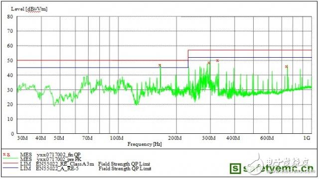
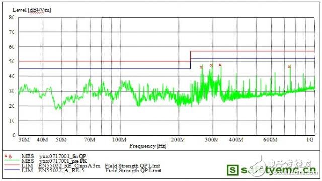
Classic case - -48V power ground is interfered by signal ground couplingA baseband frame was found to have a higher radiation at the frequency of 32.76 MHz in the RE test, and the quasi-peak value was 53.8 dB exceeding the CLASS A limit by nearly 4 dB. The results are shown in the following figure:
During the positioning process, it is found that the radiation disappears when the main control board is not inserted in the slot. As long as the main control board is plugged in, no matter how the other boards are configured, the radiation of the point exists. During the process, it was also found that a magnetic ring was stringed on the power line, and the radiation at that point also disappeared.
In order to determine the coupling path of the radiation source, the PCB of the backplane and the main control board was first examined in detail and found.
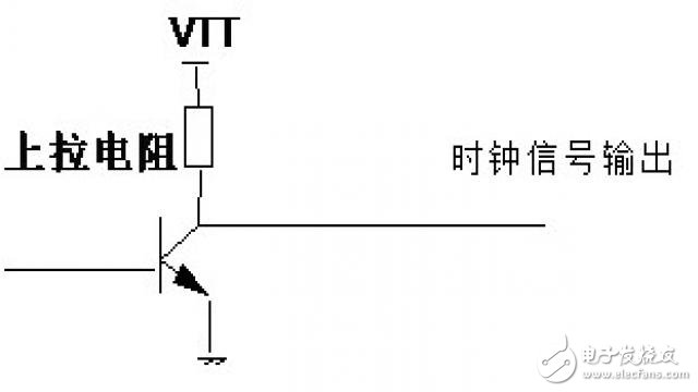
1. The cellbus clock trace is matched at both ends and matched to the VTT layer by pull-up resistors. The schematic diagram is as follows:
2. The power plane of VTT and -48V and -48V_GND has a large area overlap.
If the VTT filter capacitor selection is unreasonable, the interference may be transmitted to the VTT layer, and the VTT layer and the -48V power layer have a large area overlap on the main control board, and the -48V power layer is likely to be coupled to the interference.
Finally, it is confirmed by the positioning that after the VTT power layer is affected by CELLBUS, the -48V power layer is coupled, and then the external radiation is exceeded by the power line.
Other causes of excessive radiationWhen the radiation emission test passed, many testers liked to analyze the cause of exceeding the standard on the PCB. In addition to PCB layout and wiring, some circuit designs on the PCB can also play a decisive role in radiating emissions.
1 This circuit is the first to push the clock line matching circuit. The rising edge of the clock signal is an important factor in determining the external radiation, and the matching circuit can directly determine the signal quality of the clock. For example, for a clock circuit that matches at the beginning, improper selection of the resistors in series at the beginning or a small amount may cause large interference on the clock line.
2 decoupling circuit. The decoupling circuit on the power supply pin is also an important factor affecting the RE.
3 Other unreasonable circuits.
Classic case - PGND-GND jumper capacitor causes radiation to exceed the standard
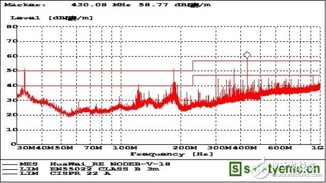
When a product is tested by RE, the 165MHz does not meet the Class A margin requirement. The test results are as follows:
View the board layout and find the layout of the ground partition as shown below:
Since the bus frequency of the board is 33MHz and the 165MHz is exactly 5 times of 33MHz, the analysis interference may be coupled from GND to PGND and driven by the network cable, resulting in excessive radiation. It can be seen from the above figure that the jumper capacitor is not directly connected between PGND and GND, but from the GND lead to PGND, and then connected to the jumper capacitor, so it is suspected that this trace will couple the interference. PGND, so that the jumper capacitor does not work. The trace is scraped off and retested. The test results are as follows:
The 165Mhz frequency disappears basically. In order to confirm whether the capacitor is connected to the ground, whether it has the same effect as the cut, the capacitor is connected to the ground and retested, and the result is still exceeded.
This case shows that the capacitor connection between GND and PGND sometimes causes the interference on the GND to couple to PGND, causing interference on the PGND and then radiating out through the cable, causing the radiation to exceed the standard.
Through years of industry work, product certification engineers have summarized a series of analysis cases on the reasons for product radiation exceeding the standard. This is the relationship between the series (4) power port and radiated emissions. The radiation exceeding the standard caused by the power supply refers to the interference inside the system that is coupled to the power line through various channels, and the device is conducted through the power line, and then radiated through the power line.
The radiated emission of the interference source to the surrounding space can be calculated according to the theory of antenna and radio wave propagation. The condition for forming the space radiation is to have a common mode driving source, and the second is to have a common mode antenna. As long as there is an RF potential difference between any two metal bodies, a pair of asymmetric vibrator antennas is formed. The noise in the system is a common mode drive source. The power cable pulled out of the cabinet can be regarded as one pole of the antenna. The common mode radiation on the power line can be approximately equivalent to the radiation of the monopole antenna. The model looks like this:
The far field distribution formula of a monopole antenna in free space is approximated as follows:
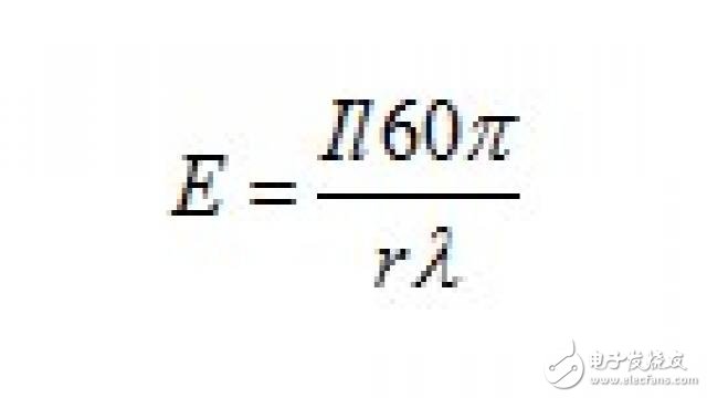
I is the current, l is the cable length, and test point r is the distance from the antenna.
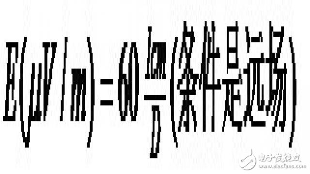
The above condition is applicable to the fact that the current distribution on the antenna is neglected and is suitable for the case where the wire is treated as a short line. This formula can be used to estimate the radiant intensity of the RE power and signal lines. Because the general cable radiation is broadband radiation, the frequency band is generally 200MHz, especially for the power line, the radiation is mainly concentrated in the tens of MHz. Taking 50MHz as an example, the corresponding wavelength is 6m, and the general power cord length is within 2m, which can basically be treated as a short line.
The current probe is clamped on the power line or signal harness of the device to measure the current on the harness, and the average value is taken into the above equation to estimate the field strength distribution in the far field.
Due to the power supply problem, there are many problems with the RE test exceeding the standard. To sum up, the specific forms of RE over-standard due to power problems are:
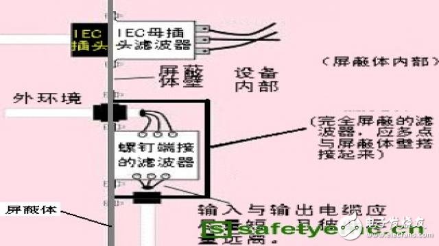
1. Filter installation problem. The filter must be installed to ensure that the filter housing is well grounded. Because the interference we want to consider is mainly vertical interference, that is, interference to the ground. Longitudinal mode interference cannot be filtered if the filter is not well grounded. Second, the installation location of the filter. As a device that suppresses conducted interference, the filter should also be used in conjunction with the case (shield). The input of the interference signal must be inside the shield. When possible, the output should be connected to the outside of the shield. In this way, interference from the inside of the casing will not be conducted through the power line, and it cannot be radiated through the space.
2. This is one of the easiest mistakes we make. It is a filtered cable that is bundled with other cables with interference or with a running wire. Due to the large distributed capacitance between the cables, the interference is easily coupled from other cables to the "clean" power line and radiated externally through the power line.
3. The power module interference is too large, or the board power circuit design is defective. Whether it is a purchased power supply or a power supply designed by itself, if the design is flawed and the interference is too large, regardless of whether the system filter meets the requirements, it may cause strong external radiation. Common problems in the design of power supply filter circuit include power supply loop problem, wrong selection of filter circuit device, filter circuit form, filter circuit position and layout (easy to generate front-to-back coupling), grounding problem of filter circuit, etc.
During the test, the most common positioning measures that the tester can take on the power port of the board is to modify the differential mode or common mode capacitor value of the filter circuit and replace the size of the common mode inductor. Generally speaking, the larger the capacitance of the differential mode and the common mode filter capacitor, the better, but the capacitance is too large, and there are problems of power-on shock and sparking and excessive leakage current; the larger the value of the filter inductor, the better, but It is also subject to flow and volume limitations.
Analysis of the cause of RE exceeding the standard caused by cableThrough years of industry work accumulation, Huaqiang Certification Network product certification engineers have summed up a series of analysis cases on the reasons for product radiation exceeding the standard. This is the series (5) cable leading to the analysis of RE over-standard causes. There is such an experience in the radiation emission test positioning process: after the first test fails, all the cables are unplugged and the test is continued. If the interference is greatly reduced without the cable, the tester needs to start from the cable analysis. The reason for the radiation exceeding the standard.
Cause of cable radiationThe radiation of the cable determines the common mode radiation. A typical cable can be thought of as a unipolar-driven antenna whose radiation field can be calculated from a simple model:
1) When the cable length l exceeds 1/4 of the operating wavelength [ie: l (m) ≥ 75 / f (MHz)], and
2) The height of the cable from the ground exceeds about 0.1 working wavelength, [ie h(m) ≥ 30/f(MHz)]
Then at this time, it can be calculated by the following formula:
Where, Icm is the common mode current (mA) and D is the distance to the receiving antenna (m).
The source of common mode interference can be divided into two parts. One is the signal converted from the differential mode signal on the cable, and the other is the common mode signal that the common mode interference source in the system is directly coupled to the cable. The reasons for the most common cable problems in the test include:
1. The cable connector is not properly connected to the chassis.
As a device that penetrates the device casing, if the connector is not properly connected to the casing, the internal interference of the system will be taken out from the inside of the casing and radiated through the cable. Due to the convincing effect, the interference source on the PCB induces a noise-like current/voltage that is as strong as a wave on the inner surface of the casing. As long as the gap above the casing is not more than 1/20 of the wavelength, we believe that these disturbances exist only in the machine. On the inner surface of the shell. As shown in the figure below, if the connector and the case are not well connected, there must be a large distributed capacitance between the surface of the connector and the inner surface of the case (because the distance is small), interference on the inner surface of the case It is easily coupled to the connector and is conducted out of the enclosure through the connector, causing external radiation on the cable.
Many design engineers believe that when the connector is designed, the connector's outer casing has been well connected to the ground on the PCB through the grounding pin, so the connector does not have to be connected to the chassis. In fact, the main purpose of connecting the shield connector to the chassis is not only a simple metal overlap, but to make the chassis form a continuous shield. It can be said that the shielding layer of the shielded cable is the extension of the shielded casing.
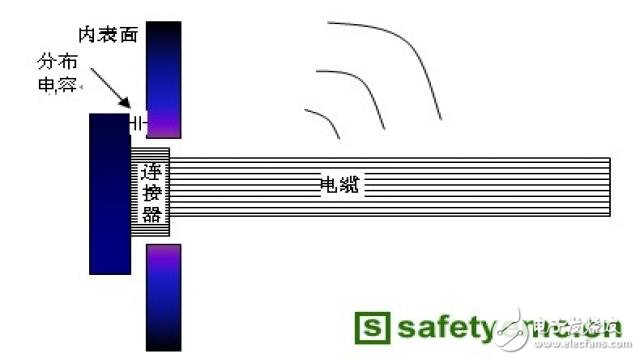
Schematic diagram of internal interference passing through the connector
When the connector is well overlapped with the inner surface of the casing, the connector and the casing form a continuous shield. It can be considered that the interference on the casing exists only on the inner surface of the shield, and the connection of the outer casing There is no interference on the device and no cable radiation will occur.
Connector lap joint good internal interference diagram
2. The cable plug housing and the cable shielding layer are not well connected.
For this reason, the radiation emission is exceeded, and the cable plug needs to be stripped and confirmed. The cable shield must be 360-degree bonded to the connector housing, and the common misconnection is that the cable designer has no sense of overlap or is only partially overlapped. It must be admitted that, especially for DB connectors, there are certain technical problems with laps. At present, we rely on the use of copper foil tape winding and welding to make the lap joint, it is easy to appear poor lap joint phenomenon. Poor overlap means that a hole is formed in the shield composed of the joint shield and the cable shield, so that interference originally present on the inner surface of the conductor leaks to the outer surface, causing external radiation.
3. Incorrect handling of the cable whose shield should be grounded at both ends.
Such cables include multi-core E1 lines, subscriber lines, and the like. During the test, ensure that the shield at the distal joint is well grounded and the distal joint is placed under the darkroom turntable to prevent external interference on the internal core. Because no matter how long the shielded cable is, the inner core wire always protrudes from the shield layer. At this time, the shield layer has a gap, and the internal interference will leak from the gap and radiate externally.

In theory, in the signal below 100KHz ~ 1MHz, in order to avoid ground loop interference, the shielded line uses single-ended grounding; and the higher frequency signal, when the cable laying length can be compared with the signal wavelength, in order to avoid standing waves Effect, the multi-point grounding method is adopted for the shielded wire. For a wideband signal cable, if both low frequency signals and high frequency signals are transmitted, mixed grounding is required in order to balance the grounding modes of different frequencies. In fact, for low-frequency signals, the external radiation itself is relatively low, and even shielded cables may not be used. The purpose of using shielded cables is to contain high-frequency external interference, and multi-point grounding should be used. It is important to note that the use of multi-point grounding can cause ground loop problems, although this problem may not be apparent in a laboratory environment.
4. Laying of signal cables.
If there is a cable with a large interference current, if there is no external radiation condition (such as a short cable length), it will not cause external radiation interference. However, if there is coupling between the cable and other cables, it may be These disturbances are coupled to the cable with external radiation conditions, causing interference. Therefore, for some cables with high interference and high interference, such as E1 cable, XDSL cable, E3 cable, 155M cable, clock cable, etc., when laying in the cabinet, it can be routed close to the cabinet shell, between the cable and the chassis. The distributed capacitance provides a low impedance interface path for high frequency interference. At the same time, separate the wires and pay attention to keep the distance from other cables.
The laying of cables for regulations not only makes people look beautiful, neat, but also benefits from reducing the coupling between cables. It should be the habit that every tester should develop.
5. The metal body does not pass through the shielded casing.
Any metal that traverses the metal shield can carry internal interference. The shielded cable does not make any overlap with the cabinet. Directly leading out of the cabinet is also a problem often overlooked by product testers in the test. It should be wrapped at the exit with a metal mesh attached to the chassis, or with a cable trunking with a wire mesh gasket. The shield of the cable is stuck.
6, other accounting defects.
If there are defects in the cable design, for example, the shielding layer has low density and poor balance; or the signal driving on the circuit is large, the signal quality is problematic, and the filter component does not meet the requirements, which may cause the cable radiation to exceed the standard.
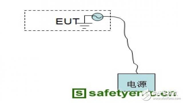
Typical case analysis1. Radiation from the grounding wire of the cabinet.
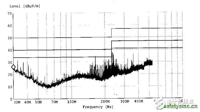
When the B product is subjected to the radiation emission test, it is found that the interference in the low frequency range of 30M to 300MHz is large under the condition that the service line only has the DC power line and the ground line, and exceeds the B level limit by about 20dBuV/m.
After investigation, the BGND and PGND of the B product are connected in the machine, and connected to the cabinet shield through a long wire AG, as shown in the following figure.
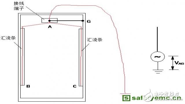
Because the AG line is long, there is a relatively large high-frequency impedance, which can effectively sense various interference signals in the machine. The cabinet housing and the grounding point A have a high-frequency voltage VAG, and the grounding line AG forms a transmitting antenna, causing the radiation emission of the whole machine to seriously exceed the standard.
Change the grounding wire to the outside of the machine. PGND is directly shorted to the cabinet, so that AG is approximately 0, that is, VAG=0, thus eliminating the antenna effect of the grounding wire and the cabinet housing. After the improvement, re-test, as can be seen from the following figure, the low-end radiation is greatly reduced, and the whole machine radiated emission is under the Class B limit line and has a 6dB margin.
This case tells us that the ground wire inside the shield must be short to ensure that internal interference is not coupled to the ground line. For shielded cabinets, the grounding point should be selected on the outer surface of the cabinet. For unshielded cabinets, the grounding point should be selected on the outer surface of the cabinet. If the inner surface must be selected, the internal wiring must be short.
2. The poor connection of the cable connector leads to excessive radiation.
The radiation emission test of a product exceeds the standard. After positioning, when the device leads the E1 line, the radiation emission test result exceeds the standard. The problem is confirmed as an E1 port problem.
After disassembling the E1 cable and the interface connector, it was found that the E1 cable shielding braid was welded to the DB68 connector metal casing only by a few wires. At high frequencies, there must be a large AC impedance on several wires, which means that an electrically continuous shield cannot be formed between the shield of the cable and the shielded casing of the device. The interference on the inner surface of the chassis can leak from the gap formed between the cable shielding layer and the chassis, and is coupled to the cable shielding layer to form external radiation.
The E1 cable shielding layer and the DB68 connector metal shell are wrapped with copper foil, and the copper foil is welded to the shielding layer, the copper foil and the copper foil, so that the copper plating and the connector are well overlapped. After processing, the test results are fully up to the limit and the margin is also met.
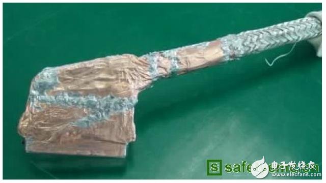
The treated E1 cable connector and shield form a whole
Plastic Package Diode.Among the electronic components, a device having two electrodes allows only the current to flow in a single direction, and many uses apply its rectification function. The Varicap Diode is used as an electronic adjustable capacitor. Most of the diodes have a current directionality that we often call the "Rectifying" function. The most common function of a diode is to allow only current to pass in a single direction (referred to as forward bias) and block in the reverse direction (referred to as reverse bias). Therefore, the diode can be thought of as an electronic version of the check valve.
Plastic Package Diode,High Frequency Diode,High Voltage Avalanche Diode,Plastic Package Zener Diode
YANGZHOU POSITIONING TECH CO., LTD. , https://www.yzpst.com