I. Heterogeneous calculation: WHY
Obviously the CPU is used well, why should we consider heterogeneous computing chips?

With the rapid growth of Internet users and the rapid expansion of data volume, the demand for computing in data centers is also rising rapidly. The demand for computing such as deep learning online prediction, video transcoding in live broadcast, image compression and decompression, and HTTPS encryption has far exceeded the capabilities of traditional CPU processors.
Historically, thanks to the continuous evolution of semiconductor technology, the throughput and system performance of computer architectures have continued to increase, and processor performance has doubled every 18 months (the well-known "Moore's Law"), enabling processor performance. Meet the needs of application software. However, in recent years, semiconductor technology improvements have reached physical limits, and circuits have become more and more complex. The development cost of each design is millions of dollars, and billions of dollars can form new product production capabilities. On March 24, 2016, Intel announced the official suspension of the "Tick-Tock" processor development model, and the future development cycle will change from a two-year cycle to a three-year period. At this point, Moore's Law is almost ineffective for Intel.
On the one hand, processor performance can no longer grow according to Moore's Law. On the other hand, data growth requires more computational performance than "Moore's Law". The processor itself cannot meet the performance requirements of HPC (High Performance Compute) applications, resulting in a gap between demand and performance (see Figure 1).
One solution is to improve processing performance through hardware acceleration and heterogeneous computing with dedicated coprocessors.
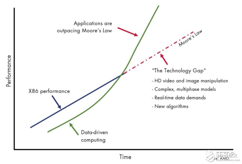
Figure 1 The gap development form for calculating demand and computing power
Second, heterogeneous calculation: STANDARDS
Usually when we provide solutions for the business, there are four choices for the deployment platform: CPU, GPU, FPGA, and ASIC. What criteria does it have to judge the pros and cons of the computing platform?
 Photo: I am a judge, I have the standard
The ideal coprocessor today should be a hardware-based design with three basic capabilities. The first is the design to provide specialized hardware acceleration to achieve the critical processing functions required in a variety of applications. Second, the coprocessor design is very flexible in performance, using pipelines and parallel structures to keep up with algorithm updates and changes in performance requirements. Finally, the coprocessor provides a broadband, low-latency interface to the main processor and system memory.
In addition to hardware requirements, the ideal coprocessor should also meet the "4P" requirements of the HPC market: performance, productivity, power, and price.
The minimum performance requirement for the HPC market is to accelerate the implementation of the algorithm, not just a single step, and to accelerate the implementation of the entire application.
Performance requirements come from the end user. In existing computer systems, the coprocessor must be easy to install, providing an easy way to configure the system and accelerate the implementation of existing applications.
The power requirements of the HPC market come from power consumption limitations in the installation and use of computing systems. For most users, there is limited space available to the computer. The lower the power consumption of the computing system, the less heat can be taken to keep the computer from overheating. As a result, low-power coprocessors can provide lower operating costs for computing systems and increase the space utilization of computing systems.
Price factors are becoming more and more important in the HPC market. More than a decade ago, the performance requirements of some applications exceeded the capabilities of a single processor, prompting the adoption of proprietary architectures such as dense parallel processing (MPP) and symmetric multiprocessing (SMP). However, such systems require the use of custom processor units and dedicated data paths, which are expensive to develop and program.
The current HPC market has abandoned such an expensive method, but instead uses a more cost-effective cluster computing method. Cluster computing uses commercial standard architectures such as Intel and AMD; industry standard interconnects such as 10 Gigabit Ethernet and InfiniBand; standard programming languages ​​such as the C language running on low-cost Linux operating systems. Today's coprocessor designs must be able to be smoothly integrated into a commercial cluster computing environment at roughly the same cost as adding another node to the cluster.
After understanding the basic criteria, we take the most popular deep learning as an example, and analyze and compare several different chips from the aspects of chip architecture, computing performance, power consumption and development difficulty.
Third, heterogeneous computing: WHICH
1, chip characteristics
The classification of commonly used processor chips has an obvious feature: CPU & GPU requires software support, while FPGA & ASIC is a software and hardware integrated architecture, software is hardware. This feature is one of the most important features of the processor chip.
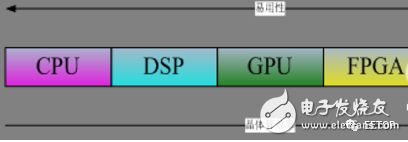
Figure 2 processor chip comparison
Figure 2 can be explained from two angles: from the direction of ASIC->CPU, the ease of use of the chip along this direction is getting stronger and stronger. The programming of CPU&GPU requires the support of the compilation system. The function of the compilation system is to put the advanced software language. Translated into instructions that the machine can recognize (also called machine language). High-level languages ​​bring great convenience and ease of use, so the software development cycle for implementing the same functions with CPU & GPU is much lower than FPGA & ASIC chips. In the direction of the CPU->ASIC, the efficiency of the transistors in the chip is getting higher and higher. Because the algorithms implemented by chips such as FPGA & ASIC are directly implemented by transistor gates, the algorithm is built directly on the physical structure compared to the instruction system, and there is no intermediate level, so the transistor is the most efficient.
Essentially, the software's operational objects are instructions, while CPU & GPUs act as high-speed execution instructions. The existence of instructions turns program execution into two parts: software and hardware. The existence of instructions also determines some completely different characteristics of various processor chips and their respective advantages and disadvantages.
The functions of FPGA & ASIC and other chips are fixed. The algorithms they implement are directly implemented by gates. Therefore, FPGA & ASIC programming is the process of implementing algorithms using gates. Software completion means that the organization of gates has been determined. In this sense, FPGA & ASIC The software is the hardware, and the software determines the organization of the hardware. The combination of hardware and software determines the extremely important resource utilization characteristics of FPGA & ASIC design. Utilization refers to the occupancy of the gate circuit resources owned by the processor in the process of implementing the algorithm by the gate circuit. If the algorithm is relatively large, there may be cases where the gate circuit resources are insufficient or although the circuit resources are sufficient, but the actual wiring difficulties cannot be performed.
There is no utilization of the processor chip CPU & GPU of the instruction system. The process by which they execute instructions is to constantly read in instructions from memory and then execute them by the executor. Since the space occupied by the memory relative to each instruction is almost infinite, even if the algorithm is huge, there is no case that the memory space is insufficient and the algorithm cannot be read. Moreover, the computer system can also be extended storage such as an external hard disk, and the instruction storage space is increased by switching the temporarily executed algorithm to the hard disk storage.
2, chip computing performance
The deep learning language, also known as Deep Neural Network (DeepNeural Networks), evolved from the Artificial Neural Networks model. We use deep learning as an entry point to analyze the performance of each chip. Figure 3 is the basic structure of a neural network. The large number of calculations for each layer in the model is the multiplication of the two matrices of the output of the previous layer and its corresponding weight value.
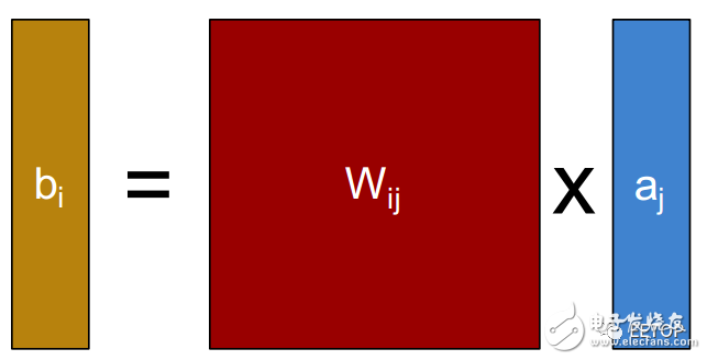
Figure 3 The basic structure of the neural network
Horizontal comparison of CPU, GPU, FPGA, ASIC computing power, the actual comparison is:
1, the multiplication and calculation ability of the hardware chip.
2. Why is there such a multiplication and calculation ability?
3. Can you give full play to the multiply-accumulate computing power of hardware chips?
With these three questions, we compare the computing power of hardware chips.
CPU computing power analysis
Here, the CPU computing power is analyzed by Intel's Haswell architecture. The computation unit on the Haswell architecture has two FMA (fused multiply-add). Each FMA can perform a multiplication operation and an addition operation on 256-bit data in one clock cycle. The corresponding 32-bit single-precision floating-point computing power is:
(256bit/32bit)* 2(FMA) * 2 (multiply and add) = 32 SP FLOPs/cycle, which means 32 single-precision floating-point calculations per clock cycle.
CPU peak floating point calculation performance = CPU core number * CPU frequency * Floating point operands executed per cycle. Intel's CPU model E5-2620V3 to calculate the peak computing power = 6 (CPU core) * 2.4GHz (CPU frequency) * 32 SP FLOPs / cycle = 460.8 GFLOPs / s 460G peak floating point computing capacity per second.
Can the CPU chip structure fully utilize the floating point calculation capability? The instruction execution process of the CPU is: fetch instruction -> instruction decode -> instruction execution. Only when the instruction is executed, the calculation unit plays a role, so that the calculation unit is not working for two periods of instruction fetch and instruction decoding. ,As shown in Figure 4.
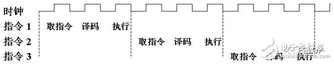
Figure 4 CPU instruction execution flow
In order to improve the efficiency of instruction execution, the CPU reads the following instructions in advance during the execution of the current instruction, so that the instructions are pipelined and the instruction execution efficiency is improved, as shown in FIG. 5. The pre-reading and pipeline execution of instructions is based on the premise that there is no correlation between instructions. How to execute an instruction does not need to wait until the result of the previous instruction is executed.
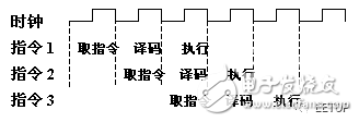
Figure 5 CPU instruction flow execution
The CPU acts as a general-purpose processor, taking into account both calculation and control. 70% of the transistors are used to build the Cache and some control units are used to handle complex logic and improve the execution efficiency of the instructions. As shown in Figure 6, the computational versatility is strong. The processing complexity is high, but the computing performance is average.
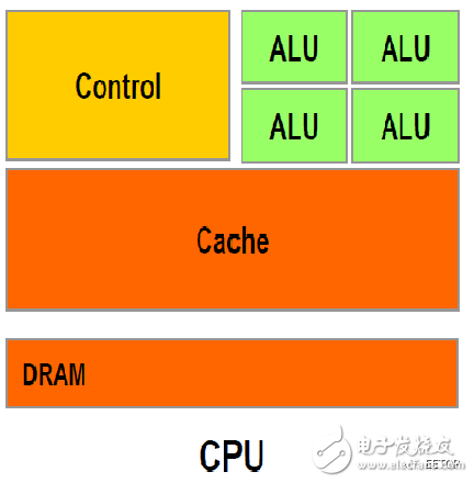
Figure 6 CPU structure
Through the CPU computing performance analysis, directly improve the computing performance direction: increase the number of CPU cores, increase the CPU frequency, modify the CPU architecture and increase the number of computing units FMA (fused multiply-add). In these three directions, directly increasing the number of CPU cores has the highest computational power, but it brings about an increase in chip power consumption and price, because only 30% of transistors in each physical core are computational units. Increasing the CPU frequency, the space for improvement is limited, and the CPU frequency is too high, which will lead to excessive power consumption and overheating of the chip. Therefore, chip manufacturers such as Intel are taking a multi-core route, which limits the frequency of a single microprocessor. Integrate multiple processor cores to improve processing performance. Modify the CPU architecture to increase the number of computing units FMA. At present, Intel follows the "Tick-Tock" two-year cycle to adjust the CPU architecture. From 2016, it will slow down to three years, and the update iteration period is longer.
GPU computing power analysis
The GPU is mainly good at parallel computing like image processing, the so-called "coarse-grain parallelism". The characteristics of graphics processing calculations are characterized by high-density calculations and less correlation between the required data. The GPU provides a large number of computational units (up to several thousand computational units) and a large amount of high-speed memory, which can simultaneously target many pixels. Perform parallel processing.
Fig. 7 is a design structure of a GPU. The starting point of the GPU design is that the GPU is more suitable for computationally intensive, multi-parallel computing. Therefore, the GPU uses more transistors for the computational unit than the CPU for the data cache and process controller. This design is because each data unit executes the same program in parallel computing, does not require cumbersome flow control and requires high computing power, and therefore does not require a large cache capacity.
Figure 7 GPU structure
A logic control unit in the GPU corresponds to multiple computing units. At the same time, if the computing units are fully paralleled, the logical control is not too complicated. The too complicated logic control can not play the parallelism of the computing unit, such as excessive if...else if ...else if... Branch computing can't increase the parallelism of the compute unit, so the logic control unit in the GPU does not need to be able to handle complex controls quickly.
Here GPU computing power is analyzed with Nvidia's Tesla K40. The K40 contains 2,880 Stream Processors, which are GPU computing units. Each stream processor contains a 32-bit single-precision floating-point multiply-and-add unit, which allows two single-precision floating-point calculations per clock cycle. GPU peak floating point performance = number of stream processors * GPU frequency * floating point operands executed per cycle. Take K40 as an example, K40 peak floating point calculation performance = 2880 (streaming processor) * 745MHz * 2 (multiply and add) = 4.29TFLOPs / s is 4.29T per second peak floating point computing power.
Can the GPU chip structure take full advantage of floating point computing power? The GPU is the same as the CPU. The instruction execution process: fetch instruction -> instruction decode -> instruction execution, the calculation unit only works when the instruction is executed. The logic control unit of the GPU is simpler than the CPU. Therefore, in order to achieve instruction pipeline processing and improve instruction execution efficiency, the processing algorithm itself must have low complexity and the processed data are independent of each other, so the serial processing of the algorithm itself will be This has led to a significant reduction in GPU floating point computing power.
FPGA computing capability analysis
As a high-performance, low-power programmable chip, FPGA can be customized according to customer-specific algorithm design. Therefore, when dealing with massive data, the advantage of FPGA compared to CPU and GPU is that FPGA is more efficient and FPGA is closer to IO.
The FPGA does not use instructions and software, and is a device that combines software and hardware. Programming the FPGA uses a hardware description language, and the logic described by the hardware description language can be directly compiled into a combination of transistor circuits. Therefore, the FPGA actually implements the user's algorithm directly with the transistor circuit, and does not translate through the instruction system.
The English abbreviated name of FPGA is translated. The full name is the field programmable logic gate array. This name has revealed the function of FPGA. It is a combination of a bunch of logic gates, which can be programmed and can be repeatedly programmed. Figure 8 shows the internal schematic of a programmable FPGA.
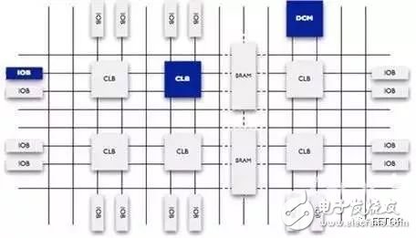
Figure 8 FPGA internal structure diagram
Here FPGA computing capability is analyzed with Xilinx's V7-690T. The V7-690T contains 3600 DSPs (Digital Signal Processing), and the DSP is the computing unit of the FPGA. Each DSP can do 2 single-precision floating-point calculations (multiply and add) per clock cycle. FPGA Peak Floating Point Calculation Performance = Number of DSPs * FPGA Frequency * Floating point operands executed per cycle. V7-690T running frequency has been calculated by 250MHz, V7-690T peak floating point calculation performance = 3600 (DSP number) * 250MHz * 2 (multiply and add) = 1.8T FLOPs / s is 1.8T peak floating point computing power per second .
Can the FPGA chip structure make full use of floating-point computing power? Because the algorithm is customized, there is no CPU and GPU instruction fetching and instruction decoding process. The data stream is directly fixed according to the customized algorithm. The computing unit can be executed every clock cycle, so the floating point can be fully utilized. Computational power, computational efficiency is higher than CPU and GPU.
ASIC computing power analysis
ASIC is a special chip, which is different from traditional general-purpose chips. A chip that is specifically tailored to a specific need. The computing power and computational efficiency of the ASIC chip can be customized according to the needs of the algorithm. Therefore, compared with the general-purpose chip, the ASIC has the following advantages: small size, low power consumption, high computing performance, high computational efficiency, and chip out The larger the volume, the lower the cost. But the disadvantages are also obvious: the algorithm is fixed and may not be usable once the algorithm changes. At present, artificial intelligence belongs to a period of great explosion, and a large number of algorithms are constantly emerging. It is far from the stationary period of the algorithm. How to adapt the various algorithms to ASIC-specific chips is the biggest problem. If the current CPU and GPU architecture are used to adapt to various algorithms, That ASIC-specific chip becomes a general-purpose chip like the CPU and GPU, and there is no advantage in performance and power consumption.
Let's take a look at the difference between FPGA and ASIC. The basic principle of FPGA is to integrate a large number of digital circuit basic gates and memory in the chip, and users can define these gates and the connection between memories by burning into the FPGA configuration file. This burn-in is not one-off, that is, the user can configure the FPGA as a microcontroller MCU today, and the configuration file can be edited tomorrow to configure the same FPGA as an audio codec. The ASIC is an ASIC. Once the design is completed, the circuit is fixed and cannot be changed.
Comparing FPGAs and ASICs is like comparing LEGO bricks and models. For example, if you find that the master of Yoda in the recent Star Wars is very hot and wants to sell a toy of Yoda Master, what do you do?
There are two ways, one is to use LEGO bricks, and the other is to find the factory to open the mold customization. If you use Lego bricks, you can buy a set of Lego bricks after designing the shape of the toy. If you are looking for a factory to open the mold, you still need to do a lot of things in designing the shape of the toy. For example, whether the material of the toy will emit odor, whether the toy will melt at high temperature, etc., so the pre-work ratio required to use Lego bricks as a toy It takes much less to find a factory for mold making, and it takes a lot faster to get from LEGO to the time it takes to get to market.
The same is true for FPGAs and ASICs. Using FPGAs, you can implement hardware accelerators with the tools provided by FPGA vendors as long as you write Verilog code. To design ASICs, you need to do a lot of verification and physical design (ESD, Package, etc.). time. If you want to target special occasions (such as military and industrial applications that require high reliability), ASICs need more time to design specifically to meet the needs, but with FPGAs you can directly buy military-grade high-stability FPGAs. Affect development time. However, although the design time is relatively short, the toys made by Lego bricks are rougher (poor performance) than the factory-customized toys (after the picture below). After all, the factory mold opening is tailor-made.

In addition, if the shipment is large, the cost of mass production of toys in the factory will be much cheaper than using LEGO bricks. The same is true for FPGAs and ASICs. At the same time, the accelerator of the ASIC implemented with the best process will be 5-10 times faster than the accelerator with the same process FPGA, and the cost of the ASIC will be far after mass production. Lower than the FPGA solution.
The speed of FPGA is fast, the speed of ASIC is slow, it takes a lot of time to develop, and the one-time cost (lithographic mask fabrication cost) is much higher than that of FPGA, but the performance is higher than FPGA and the average cost after mass production is lower than FPGA. In terms of target markets, FPGAs are costly, so they are suitable for places that are not very price sensitive, such as enterprise applications, military and industrial electronics, etc. (reconfigurable in these areas is really needed). ASICs are suitable for consumer electronics applications due to low cost, and whether configurable in consumer electronics is a pseudo-demand remains to be discussed.
The same is true of the market situation we see: the use of FPGAs for deep learning acceleration is mostly for enterprise users. Companies such as Baidu, Microsoft, and IBM all have FPGA-specific teams that accelerate servers, and the target market for Teradeep, a startup that makes FPGA solutions. It is also a server. ASICs are primarily aimed at consumer electronics, such as Movidius. Since the mobile terminal belongs to the field of consumer electronics, the solution for future use should be ASIC-based.

3, platform performance and power consumption comparison
Due to different chip production processes, the power consumption and performance of the chip are affected. Here, the same process or close to the process is used for comparison. The ASIC chip has no commercial chip, and Google's TPU only uses its own information. Here, the ASIC chip is represented by "DianNao: A Small-Footprint High-Throughput Accelerator for Ubiquitous Machine-Learning" published in an academic paper.

From the above comparison, the energy consumption ratio: ASIC > FPGA > GPU > CPU, the root cause of such a result: for computationally intensive algorithms, the higher the energy consumption ratio of data moving and computing efficiency. Both ASIC and FPGA are closer to the underlying IO, so the computational efficiency is high and the data is moved high, but the FPGA has redundant transistors and wires, and the operating frequency is low, so there is no ASIC energy consumption ratio. Both the GPU and the CPU belong to the general-purpose processor, and all need to perform the process of instruction fetching, instruction decoding, and instruction execution. In this way, the processing of the underlying IO is shielded, so that the hardware and software are decoupled, but the data is moved and operated. No higher efficiency can be achieved, so there is no ASIC or FPGA energy consumption ratio. The difference in power consumption between the GPU and the CPU is mainly due to the fact that most of the transistors in the CPU are used in the cache and control logic units, so the CPU has redundancy for computationally intensive algorithms with low computational complexity compared to GPUs. The transistor does not work and consumes less power than the CPU on the GPU.
Fourth, summary and outlook
In the long-term development process of the processor chips, some characteristics of use and market are formed. There are a large number of open source software and application software in the CPU & GPU field. Any new technology will first implement the algorithm with the CPU, so the CPU programming resources are rich and easy to obtain, and the development cost is low and the development cycle. The implementation of FPGA is implemented by the underlying hardware description language such as Verilog/VHDL. The developer needs to have a deep understanding of the chip characteristics of the FPGA, but its high parallelism can often improve the performance of the business. At the same time, the FPGA is dynamic. Reconfigurable, after being deployed in the data center, different logics can be configured according to the service form to implement different hardware acceleration functions; for example, the FPGA board on the current server deploys image compression logic to serve QQ services. At this time, the real-time prediction of the advertisement needs to be expanded to obtain more FPGA computing resources. Through a simple FPGA reconfiguration process, the FPGA board can be transformed into a “new†hardware to serve real-time advertising prediction, which is very suitable for batch deployment. ASIC chips can achieve optimal performance, that is, high area utilization, high speed, and low power consumption; however, AISC has great development risks, requires a large enough market to guarantee cost price, and has a long time period from R&D to market. It is not suitable for areas where algorithms such as deep learning CNN are rapidly iterating.
Speaking so much, when you encounter a business bottleneck that requires heterogeneous computing chips, can you choose the right chip based on business characteristics and chip characteristics?
After analyzing all kinds of chip characteristics, the next step is to come!

Today's FPGAs have great performance potential, support for deep variable pipeline structures, provide a large amount of parallel computing resources, and perform very complex functions in one clock cycle. The programmability of the FPGA ensures that the device meets the specific needs of the application software, without the cost or latency of designing a custom coprocessor. The FPGA is reprogrammable, providing very flexible custom co-processing for multiple applications on a single chip. With an FPGA, the business has unlimited possibilities. The same semiconductor technology can not only maximize the performance of the processor, but also enable the FPGA to evolve from a simple glue logic controller to a high performance programmable architecture. FPGAs are fully capable of meeting the "4P" needs of the HPC market.
The built-in memory of the FPGA also has great performance advantages. For example, on-chip memory means that the memory access bandwidth of the coprocessor logic is not limited by the number of device I/O pins. Moreover, the combination of memory and operational logic eliminates the need for external high-speed memory buffering. This also avoids buffered access and consistency issues with high power consumption. Using internal memory also means that the coprocessor does not require additional I/O pins to increase its accessible memory capacity, simplifying the design.
Many people are skeptical because of the difficulty in developing FPGAs and the long development cycle. The good news is that HLS and OpenCL languages ​​are getting better and better, and many applications can achieve greater performance improvements by directly using these two high-level languages.
- The Description of TV Antenna
-
In the cable TV system, the task of the antenna is to receive the open channel TV signal or satellite TV signal in the air, and send it to the system for processing, transmission and distribution. Among them, the antennas receiving VHF and UHF open-circuit TV signals are called TV receiving antennas.
- TV receiving antenna is an important part of wireless TV signal receiving, and it is the gate for radio waves to enter the CATV system. There are two kinds of antenna: passive antenna and active antenna. The active antenna can make the antenna system realize high gain and high signal-to-noise ratio receiving.
The Picture of TV Antenna


TV Antenna outdoor,TV Antenna Indoor,TV Antenna at best buy,TV Antenna Booster,TV Antenna Amazon
Yetnorson Antenna Co., Ltd. , https://www.xhlantenna.com