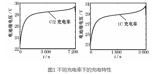
The nominal nickel-hydrogen battery has a nominal voltage of 1.2v and a charge termination voltage of 1.5v; the discharge termination voltage is typically 1.1v. The charging characteristics of NiMH batteries are affected by the charging current, temperature and charging time. "The battery terminal voltage increases with the increase of the charging current, and the closer to the maximum value, the faster the temperature of the battery rises, and the more susceptible the battery is damaged. The charging current is greater than “0.5C (C indicates the battery charging rate), the terminal voltage of the battery reaches the maximum voltage faster, and the charging and discharging capacity will become smaller, resulting in a decrease in battery performance.
The charging characteristics of 24V/10Ah NiMH batteries at different charging rates are shown in Figure 1.
1. The charger has various functions such as pulsation current limiting charging, trickle charging, and charging self-stop. Thereby achieving intelligent charging, no need to be taken care of.
2. The charger is triggered by the residual power of the battery. When the battery is not connected, there is basically no voltage output; only when the battery is properly connected, the charging current is output. With short circuit protection or reverse connection protection.
3. The circuit has strong applicability and is characterized by: (1) wide input voltage range; (2) it can be adapted to charge other types of rechargeable batteries as long as the potentiometer is adjusted, (3) at the output of the circuit and by a filter capacitor, the circuit can become a PWM The way the adjustable DC regulated power supply.
Circuit schematic: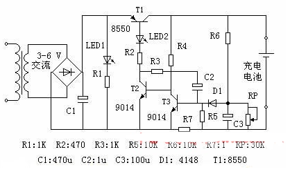
This circuit is designed for single-cell NiMH batteries. As shown in the figure: the mains is transformed by a transformer, rectified by a full bridge, and the capacitor C1 is filtered to become a direct current. LED1 is the power indicator, LED2 is the charging indicator, T1 is the charge control transistor, and works in the switch state; T2, T3 and capacitor C2 form a one-shot. R6 and RP form a voltage limiting sampling circuit, and R7 is a current limiting sampling resistor.
standby mode:When the power is turned on, if the battery is not connected, the transistor T2 is turned off due to the absence of the base voltage, and the transistor T1 is also turned off, and no voltage is output. At this time, only the power indicator LED1 is illuminated.
Charging process:When the rechargeable battery is properly connected, the transistor T2 is slightly turned on due to the residual power of the battery, its collector potential drops, T1 turns on quickly, and the output voltage rises; since C2 is positive feedback, the circuit state quickly reaches steady state. At this time, T1T2 is turned on, T3 is turned off, the battery is charged, and the charging indicator LED2 is illuminated.
Current limiting charging:If the charging current is greater than the limit value, the voltage across the current sampling resistor R7 rises, and the voltage between the BE poles of the transistor T3 is higher than the deadband voltage, and the one-shot trigger state is triggered. T3 is turned on, T1T2 is turned off, charging is stopped; then the one-shot trigger is automatically reset, and then enters the charging state, so that the pulsating charging is performed repeatedly. The charging indicator LED2 flashes. Charging self-stop: As the charging progresses, the voltage across the battery rises slowly, the pulse width becomes narrower, the charging current becomes smaller, and the charging indicator LED2 flashes gradually and becomes darker. When the battery is nearly full, the diode D1 is turned on, T3 is also turned on, T1T2 is turned off, the charging circuit is turned off, and charging is ended. In the actual charging process, after the battery is left to stand for a while, the battery voltage is slightly lowered, so intermittent charging may occur, but the LED 2 may not be blinking. This trickle charge method helps to extend battery life.
Installation and commissioning:After the installation is correct, follow the steps below to debug: disconnect the capacitor C2C3, and connect an electrolytic capacitor of about 220uF at the output end. At this time, the circuit is equivalent to an adjustable regulated power supply. Do not connect the battery, turn on the power, LED1 emits light, short the T3, b, e poles, the charging indicator LED2 should be on, use the multimeter to measure the output voltage, adjust the potentiometer RP until the output voltage is equal to the final voltage of the rechargeable battery Then connect the capacitor C2C3. (The battery charging voltage can be checked from the data or can be measured; for example, the voltage of a single NiMH battery is about 1.4V, and the single cell is about 2.45V.).
Nickel-metal hydride battery charger production method 2The design circuit is shown in the figure below: It uses the principle of series charging to charge 1~4 nickel-metal hydride batteries. The utility model has the advantages that different connection lines can be made, and the charger output end is directly connected to the charging socket of the electric appliance for charging, and the battery is not necessary to be disassembled and then charged into the battery clip of the charger, which is particularly convenient in use.
Principle of charging processIts charging curve is shown in the waveform on the right side of Figure 1. When charging starts, it charges the battery for 4.4 hours with a constant current of 0.3C (C is the battery capacity divided by the current value of 1 hour), and then automatically turns to 0. The smaller current of the O96C continues to charge the battery for 2.2 hours and then to the continuous trickle charge of lOrnA. The advantage of this design is that it avoids the high heat generated by the battery when it is near full, which prolongs the battery life. In the first stage of charging, there is a 1/10 time to stop charging, and during this time a high current discharge pulse of about 5 ms is inserted, as shown in the lower right waveform. The reciprocal insertion of this discharge pulse can remove the polarization caused by the large current charging, and the charging efficiency is higher. Practice has proved that this method can improve the cleanliness of the battery, increase the total charge and discharge times of the battery, and have a certain recovery capacity for some old batteries, which is better than the stable constant current charging effect.
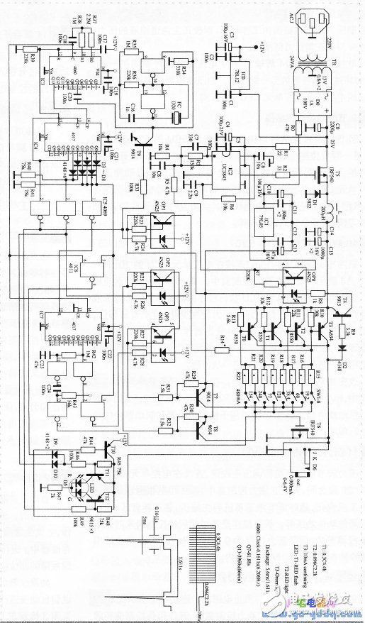
The principle of the design is shown in Figure 1. The 220V/AC power supply is stepped down by the transformer TR to become 13V/0.8Ax2 AC. After rectification by the rectifier bridge DO, the capacitors CO, RO, C1O are filtered to become +15V/1A and - 13V/0.1A two sets of voltage. The integrated block IC2 and the power MOS transistor T5 form a typical switching regulator source, which can obtain a stable power supply of 1.2~7.6V/1A on C14 and C15.
The sampling design of this circuit is unique. It does not directly sample the output voltage. Instead, it measures the voltage dropped on the e and c junctions of the charge control transistors TO~T3 through T4, R9, and D2, and then passes through R8 and optocoupler OPO. Control the sampling terminal of IC2 so that the transistor junction voltage is constant at 1.2V. That is, the output voltage of the circuit is varied, it can automatically track the voltage of the charging output terminal, and ensure that the operating voltage of the control transistor is constant. The purpose of adding a switching power supply is to improve the power efficiency of the charger, so that the actual efficiency of charging one battery and four batteries is not changed much, and the device is prevented from generating high heat.
The three-terminal regulated power supply ICO provides +12V/0.1A working power to digital control circuits. The negative three-terminal regulated power supply IC1 is designed for constant genre circuits and outputs an auxiliary power supply of -5V/0.1A (for the output of the switching power supply). The charging switch and constant current control are carried out by 4 transistors TO~T3. Each transistor is only responsible for outputting a certain current at a time, thus avoiding the constant current accuracy caused by the linearity of the device when using a single control tube. decline.
SW1~8 is 1&TImes; 8D1P switch, which consists of 4 levels of binary current value control, which are 480-240-120-60mA and 154-77-38.4, -19.2mA respectively. The first set of switches controls the first stage charging current and the second set of switches controls the second stage charging current. T7, T8 and OP1~OP3 form a switch interface circuit, which respectively control the opening and closing of the circuit and the conversion of charging at different stages.
The reason why the photocoupler is used here is that the voltage on the main circuit is variable, and the ordinary interface circuit cannot be used for control. The digital circuit IC3 (4060) is an oscillating frequency divider. The oscillating signal of 6.206 Hz generated by the multi-stage frequency division outputs 61.88 s (cycle) on Q7 and 3960 s (cycle) on Q13. The signal is distributed by the pulse of IC4 (4017) and the OR logic of diodes D3~D8, forming a 4L 4 hour first stage timing signal and a 2.2 hour second stage timing signal, as well as Q6 output charging. End signal.
The output of Q6 is fed back to the CE terminal, so that when Q4 of IC4 outputs a high level, the input is blocked and the state is maintained. The function of C17 and R39 is to clear IC3 and IC4 at the moment of power-on, and to ensure the timing starts from the beginning. The signal generated by the QO~Q34 outputs of IC4 passes through the OR gate of D3~D6 to the IC5(1) pin, and the IC6(1) and (5) pins provide high level, which makes the output of IC5(2) pin low. The level makes the R terminal of IC7 low, and IC7 starts to work. Together with IC1's (1), (2), and (2) NAND gates, it generates a one-stage constant current charging intermittent control signal through OP3. And T7 controls TO~T3 and enters the first stage of charging.
At the same time, the (4), (5), (6) and NAND gate (5) pins of IC6 have reached a high level, (6) the pin receives the oscillation signal from IC3, and the (6) pin outputs a 6.206 Hz square wave. The red diode in the two-color LED is controlled to flash by D9 and T11, indicating the first stage charging. During this period, the CP terminal of IC7 also receives the oscillation pulse from IC3, and generates a high-level signal with a duty ratio of 1/10 on its Q3 output. It passes through R42, C23 integration circuit, R43, C24 differential circuit and The two inverters in IC5 generate a discharge control signal with a value of about 5 ms, and directly drive the discharge MOS transistor T6 to form a large current discharge pulse.
In the second stage of charging, the Q4 and Q5 terminals of IC4 output a high level, and after IC5(3), (4) inverters, output low level, one way through OP2, T8 control constant current circuit to convert current, the other way The LEDs are constantly red-emitting through D1O and T11, indicating the second-stage charging. At this time, the R terminal of IC7 has been placed at a high level. The Q3 terminal is constantly at a zero level, the discharge circuit has stopped working, and there is no pause in the charging waveform, which becomes a stable constant current charging.
At the end of the second phase of charging, IC4's Q6 output is high. After IC5(5), (6) is reversed, OP1 is controlled, the inverted choke circuit generates 1OmA of turbulent current, and the LED is controlled by Tl2. Light, indicating the end of the second phase of charging. The signal also turns off T9 through R33, so that the Q7 output of IC3 passes through the C20, R34 differential circuit enable two NAND gates in IC6 to form a square wave generator, which generates a "61.88s" on the piezoelectric sheet FC.嘀", prompting the user that the charging process has ended.
Drop Cable,Fiber Drop Cable,Bus Drop Cable,Fiber Optic Drop Cable
Huizhou Fibercan Industrial Co.Ltd , https://www.fibercan-network.com