Ask a question
Can I turn the RF source on or off within 200 ns?
In pulse radar applications, high power amplifiers (HPAs) need to be turned on/off quickly during the transition from transmit to receive. Typical conversion time targets may be less than 1 μs. Traditionally, this is achieved through drain control. Drain control requires switching large currents from 28 V to 50 V. Switching power technology is known to perform this task, but involves additional physical size and circuit issues. In modern phased array antenna development, while requiring as low a SWaP (size and power consumption) as possible, it is desirable to eliminate the complexities associated with HPA drain switches.
This article will present a unique but simple gate pulse drive circuit that provides an alternative method for fast switching HPA while eliminating the circuitry associated with the drain switch. The measured switching time is less than 200 ns, and there is some margin relative to the 1 μs target. Other features include offset programming to resolve differences between devices, gate clamping to protect the HPA from gate voltage increases, and overshoot compensation to optimize pulse rise time.
Typical drain pulse configuration
A typical configuration of the HPA through the drain control switch is shown in Figure 1. A series FET turns on the high voltage of the input HPA. The control circuit needs to convert the logic level pulse to a higher voltage to turn the series FET on.
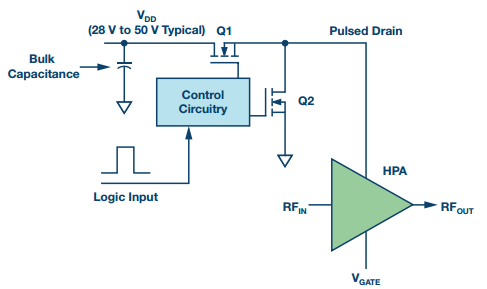
Figure 1. Traditional HPA pulse drain configuration
Difficulties in this configuration include:
✦ High current switching requires a low inductance path from the bulk capacitor to the HPA drain pin.
æ¼æž When turned off, the drain capacitor holds charge and requires an additional discharge path. This is achieved with an additional FET Q2, and the constraints on the control circuit increase: Q1 and Q2 must not be enabled at the same time.
✦ In many cases, the series FET is an N-channel device. This requires the control circuit to generate a voltage higher than the HPA drain voltage to turn it on.
The design method of the control circuit is well known and effective. However, phased array systems continue to expect integrated packaging and reduce SWaP, so it is desirable to eliminate the above difficulties. In fact, people's desire is to completely eliminate the drain control circuit.
Recommended gate pulse circuit
The goal of the gate drive circuit is to convert the logic level signal to a suitable GaN HPA gate control signal. A negative voltage is required to set the proper bias current and a larger negative voltage to turn off the device. Therefore, the circuit should accept a positive logic level input and convert it to a pulse between two negative voltages. The circuit also needs to overcome the effects of gate capacitance, providing a rapid rise time, and the overshoot should be minimal or absent.
A concern with the gate bias setting is that a small increase in bias voltage can result in a significant increase in HPA current. This adds to the goal that the gate control circuit should be very stable and have a clamp to prevent damage. Another problem is that the optimum bias voltage for different devices is different when setting the required drain current. This difference makes it more desirable to have in-system programmable gate bias characteristics.
The circuit shown in Figure 2 achieves all of the stated objectives. Operational amplifier U1 uses an inverting single negative supply configuration. The op amp reference is set with a precision DAC to achieve the gain on the V+ pin. When the logic input is high, the op amp is clamped to the negative supply rail. When the input is low, the op amp output approaches a small negative value determined by the resistor value and the DAC setting. The inverting configuration is deliberately chosen to turn on the HPA when the logic input is low or grounded because the voltage difference of the logic low is less than the logic high. A rail-to-rail operational amplifier with high slew rate and sufficient output current drive capability is suitable for this application.
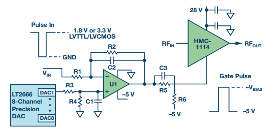
Figure 2. Recommended HPA gate drive circuit
The component values ​​are selected as follows:
â—† R1 and R2 set the op amp gain.
â—† The DAC setting along with R3 and R4 determines the reference voltage for the op amp's V+ pin. C1 and R3 are selected for low pass filter noise.
◆ R5 and R6 are used to implement important clamping functions. This is because the op amp's VCC pin is ground-referenced, so this is the maximum value of the op amp's output. R5 and R6 provide a resistor divider for the –5 V supply.
â—† The adverse effect of R5 is due to the gate capacitance, which slows down the impulse response. This is compensated by adding C3 to achieve a steep pulse.
â—† The value of C2 is small to limit the overshoot of the rising edge of the op amp output pulse.
actual data
The test setup for the verification circuit is shown in Figure 3. Use evaluation boards for precision DACs, op amps, and HPA. A pulse generator is used to simulate a 1.8 V logic signal. The signal generator operates continuously and measures the on/off of the RF signal by the HPA using an RF sampling oscilloscope with an input bandwidth higher than the RF frequency.
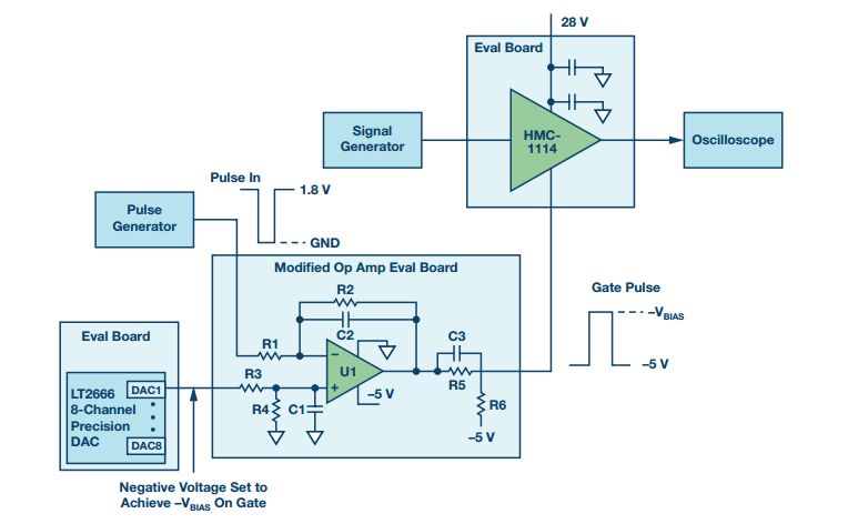
Figure 3. Test setup
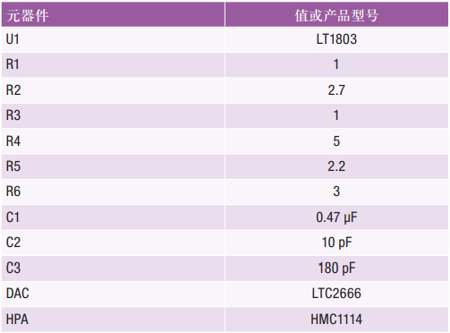
See Table 1 for the component values ​​used for the test.
Table 1. Component values ​​used
The measured turn-on time is shown in Figure 4. The time scale is 500 ns per cell and the rise time of the RF signal is less than 200 ns. For systems that measure the time from the start of the gate pulse to the end of the rising edge of the RF pulse, it can be seen that the turn-on time is approximately 300 ns, which indicates that the system allocates 1 μs for a considerable amount of margin for transmit-to-receive conversion.
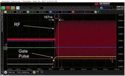
Figure 4. Measured HPA turn-on time
The measured off time is shown in Figure 5. The time scale is also 500 ns per division, and the fall time is significantly faster than the rise time, which is also much less than 200 ns, indicating that the system allocates 1 μs for a considerable amount of margin for transmit-to-receive conversion.
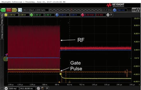
Figure 5. Measured HPA shutdown time
Layout considerations
A dimensional study of a representative layout is shown in Figure 6. The op amp portion of the gate pulse circuit is placed near the RF path to the HPA input. The precision DAC is not shown, it is assumed to be placed in the control section to provide input for multiple transmit channels. Layout studies have shown that this circuit can be added to an actual low-cost PWB implementation with minimal additional space required to transmit RF circuitry.
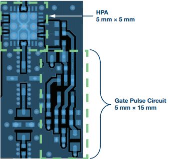
Figure 6. Physical size allocation
Conclusion
This paper presents a unique gate pulse circuit and performs HPA fast on/off evaluation. Its features include:
è½¬æ¢ Conversion time is less than 200 ns.
兼容 Compatible with any logic input
消除 Eliminate device-to-device differences with programmable offsets
✔ Provide clamp protection to set the maximum gate voltage
ä¸Šå‡ Rise time / overshoot compensation
✔ Size support for high density phased array applications
The increasing integration of advanced electronic systems requires a reduction in physical size, so it is conceivable that other changes to this circuit and its methods will begin to proliferate in phased array applications that require fast HPA conversion times.
Vecsel Gain Chip,Laser Gain Chip,Laser Diode On A Chip ,Laser Diode Junction
AcePhotonics Co.,Ltd. , https://www.acephotonics.com