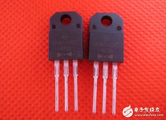
Schottky diodes are named after their inventor, Dr. Schottky, short for Schottky Barrier Diode (abbreviated as SBD). The SBD is not fabricated by the principle of forming a PN junction by contacting a P-type semiconductor with an N-type semiconductor, but by a metal-semiconductor junction principle formed by metal-to-semiconductor contact. Therefore, SBD is also called a metal-semiconductor (contact) diode or a surface barrier diode, which is a hot carrier diode.
The Schottky diode is a metal-semiconductor device in which a noble metal (gold, silver, aluminum, platinum, etc.) A is a positive electrode, and an N-type semiconductor B is a negative electrode, and a barrier formed on the contact surface thereof has a rectifying property. Since there are a large number of electrons in the N-type semiconductor, and there is only a very small amount of free electrons in the noble metal, the electrons diffuse from the high concentration B to the low concentration A. Obviously, there is no hole in the metal A, and there is no diffusion movement of holes from A to B. As electrons continue to diffuse from B to A, the electron concentration on the B surface gradually decreases, and the surface electrical neutrality is destroyed, thus forming a potential barrier whose electric field direction is B→A. However, under the action of the electric field, the electrons in A also produce a drift motion from A→B, thereby weakening the electric field formed by the diffusion motion. When a space charge region of a certain width is established, the electron drift caused by the electric field and the electron diffusion motion caused by the difference in concentration reach a relative balance, and a Schottky barrier is formed.
The internal circuit structure of a typical Schottky rectifier is based on an N-type semiconductor on which an N- epitaxial layer using arsenic as a dopant is formed. The anode is made of a material such as molybdenum or aluminum to form a barrier layer. Silica (SiO2) is used to eliminate the electric field in the edge region and increase the withstand voltage of the tube. The N-type substrate has a small on-state resistance, and its doping concentration is 100% higher than that of the H-layer. An N+ cathode layer is formed under the substrate to reduce the contact resistance of the cathode. By adjusting the structural parameters, a Schottky barrier is formed between the N-type substrate and the anode metal as shown. When a forward bias is applied to both ends of the Schottky barrier (anode metal is connected to the positive electrode of the power supply, and the N-type substrate is connected to the negative electrode of the power supply), the Schottky barrier layer is narrowed, and the internal resistance becomes small; When a reverse bias is applied across the Schottky barrier, the Schottky barrier layer becomes wider and its internal resistance becomes larger.
In summary, the structural principle of the Schottky rectifier is very different from that of the PN junction rectifier. The PN junction rectifier is usually called a junction rectifier, and the metal-semiconductor rectifier is called a Schottky rectifier. Aluminum-silicon Schottky diodes fabricated using a silicon planar process have also been introduced, which not only saves precious metals, significantly reduces costs, but also improves parameter consistency.
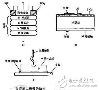
The structure and materials of the new high-pressure SBD are different from those of traditional SBD. A conventional SBD is formed by contacting a metal with a semiconductor. The metal material may be aluminum, gold, molybdenum, nickel, titanium or the like, and the semiconductor is usually silicon (Si) or gallium arsenide (GaAs). Since electrons have a larger mobility than holes, in order to obtain good frequency characteristics, an N-type semiconductor material is selected as the substrate. In order to reduce the junction capacitance of the SBD and increase the reverse breakdown voltage without making the series resistance too large, a high-resistance N-thin layer is usually epitaxially grown on the N+ substrate. The structure diagram is shown in Fig. 1(a), and the graphic symbols and equivalent circuits are shown in Fig. 1(b) and Fig. 1(c), respectively. In Figure 1(c), CP is a shrouded capacitor, LS is the lead inductance, RS is a series resistor including the semiconductor body resistance and lead resistance, and Cj and Rj are the junction capacitance and the junction resistance, respectively. The function of the bias voltage). As you know, there are a large number of conductive electrons inside the metal conductor. When the metal is in contact with the semiconductor (the distance between them is only on the order of the atomic size), the Fermi level of the metal is lower than the Fermi level of the semiconductor. The electron density is smaller than the electron density of the semiconductor conduction band at the sub-level corresponding to the semiconductor conduction band inside the metal. Therefore, after the contact between the two, electrons diffuse from the semiconductor to the metal, causing the metal to carry a negative charge and the semiconductor is positively charged. Since metal is the ideal conductor, the negative charge is only distributed within a thin layer of atomic size. For an N-type semiconductor, a donor impurity atom that loses electrons becomes a positive ion and is distributed in a large thickness. As a result of the diffusion of electrons from the semiconductor to the metal, a space charge region, a self-built electric field and a barrier are formed, and the depletion layer is only on the side of the N-type semiconductor (the barrier regions all fall on the semiconductor side). The direction of the self-built electric field in the barrier region is directed to the metal by the N-type region. As the thermal electron emission increases from the built field, the drift current opposite to the direction of the diffusion current increases, eventually reaching dynamic equilibrium, forming a contact potential between the metal and the semiconductor. Base, this is the Schottky barrier.
When the applied voltage is zero, the diffusion current of the electron is equal to the reverse drift current, achieving dynamic balance. When a forward bias is applied (ie, a positive voltage is applied to the metal, and a negative voltage is applied to the semiconductor), the self-built field is weakened, and the barrier on the semiconductor side is lowered, thereby forming a forward current from the metal to the semiconductor. When reverse bias is applied, the self-built field is enhanced and the barrier height is increased to form a small reverse current from semiconductor to metal. Therefore, the SBD, like the PN junction diode, is a nonlinear device with unidirectional conductivity.
A manual pulse generator (MPG) is a device normally associated with computer numerically controlled machinery or other devices involved in positioning. It usually consists of a rotating knob that generates electrical pulses that are sent to an equipment controller. The controller will then move the piece of equipment a predetermined distance for each pulse.
The CNC handheld controller MPG Pendant with x1, x10, x100 selectable. It is equipped with our popular machined MPG unit, 4,5,6 axis and scale selector, emergency stop and reset button.
Manual Pulse Generator,Handwheel MPG CNC,Electric Pulse Generator,Signal Pulse Generator
Jilin Lander Intelligent Technology Co., Ltd , https://www.jilinlandertech.com