With the improvement of people's living standards, the number of private vehicles on the road has also increased, but the problem that comes with it is that the traffic accident rate is high, which seriously endangers people's lives. In this paper, how to prevent traffic accidents, research and design a vehicle that is responsive, reliable, and economical. The key task of the equipment in the design process is to use high-speed acquisition of the lidar echo signals at the left and right ends of the vehicle head and store and process the laser radar echo signals in real time, so as to quickly measure the distance between the vehicle and the obstacles. And relative speed.
1 System OverviewFor the radar system used in highways, considering that the speed of driving is relatively fast, it is unable to respond immediately to some unexpected events. Therefore, it is required to design the anti-collision radar to detect the distance as long as possible, so that the driver can advance the driver. Prepare for safety, so this highway collision avoidance system generally uses laser detection. The structure of the car collision avoidance system using laser ranging is shown in Figure 1.

For the electrical signal formed by the laser radar echo signal after photoelectric device conversion, the signal frequency is high, the pulse width is relatively narrow, the signal amplitude is low, and the background noise is large. If the low-speed data acquisition system is used for data acquisition, then There will be insufficient data accuracy, so a high sampling rate, high resolution data acquisition system must be used. The overall principle block diagram of the system is shown in Figure 2.
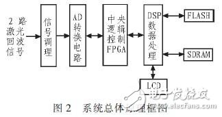
The main signal flow of the system: the 2-channel lidar echo signal obtained by the laser sensor is firstly conditioned by buffer amplification, and then sent to the AD conversion circuit for analog-to-digital conversion, and then simultaneously collected by the central logic control module FPGA. This greatly improves the speed compared to the time-sharing acquisition with the DSP. On the one hand, FPGA completes the sampling control of A/D, on the other hand, it forms a transmission channel with the EMIF interface of DSP, completes the data transmission task between AD and DSP, avoids the direct communication between ADC and DSP, and reduces the large amount of data. The pressure of transmission.
2.1 front-end signal conditioning circuit
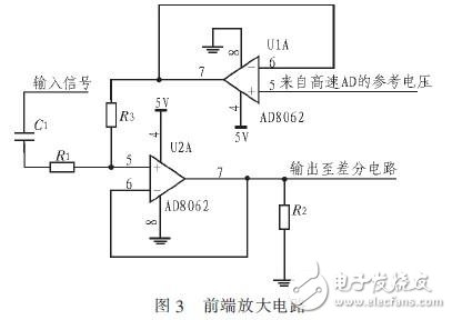
2.1.1 Front end amplifier circuit
The signal output from the sensor must be conditioned to effectively collect data. In order to achieve the highest measurement accuracy, the voltage range of the signal under test should be amplified to the vicinity of the maximum ADC range. Therefore, the small signal from the sensor needs to pass through the front end. The amplifying circuit is linearly amplified to an electrical signal suitable for the system. In this system, the low-cost op amp module of AD8062 produced by AD company is mainly used, as shown in Figure 3.
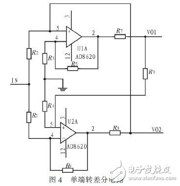
2.1.2 Front-end differential circuit
In order to eliminate the even harmonic component, suppress the common mode noise source, and play the anti-interference effect of the system, the AD conversion circuit of the system adopts the form of differential input, and the signal obtained by the amplifying circuit is a single-ended signal, so The input single-ended signal of the front end is converted into a differential signal. This design selects the AD8620 driver chip produced by Analog Devices to form a differential drive circuit. The specific circuit design is shown in Figure 4.
2.2 AD conversion circuit
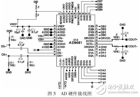
In the data acquisition system, AD is a relatively important link, mainly to complete the collection of laser echo signals, and the sampling clock signal can be provided by the clock module inside the FPGA circuit. Analog Devices' AD9481 can use a differential input with a sampling rate of 250 MSPS and a 250 M PECL standard clock signal. To create this differential clock signal, consider the MC100LEL16 clock chip. The digital output of the AD9481 is a parallel interface with a 16-bit data stream. For such high-speed data and storage, there is a competitive risk and the system is unstable. Therefore, a 100 Ω is connected in series between the output of the AD and the FPGA at the design time. The resistance can eliminate the interference between the glitch and the high-speed data line between 0 and 1. The specific AD hardware principle is shown in Figure 5.
2.3 data processing part of the hardware circuit
The data processing part of this system is completed by two parts of FPGA and DSP. According to the signal output timing of the previous AD circuit, VHDL programming is performed to realize the acquisition of the digital signals of the two AD outputs at the same time, input the data into the FIFO module, and then quickly transfer the data to the DSP through the EMIF bus to perform related algorithms. The operation.
2.3.1 FPGA Circuit
FPGA uses hardware programming to implement complex logic functions. It not only can preprocess the collected large-volume data stream, but also provides the clock signal required by the system as the core part of the whole control system to ensure the orderly collection of data. The link of data transmission ensures the data transmission between AD and DSP. Combined with sampling, storage and other functions, the FPGA module is mainly divided into four parts: clock management module, A/D control module, FIFO buffer module, and EMIF interface module with DSP:
1) Clock management module, this part is mainly to generate the clock signal of each module required by the system. This system is realized by the DCM module that comes with ISE software.
Changshu Herun Import & Export Co.,Ltd , https://www.herunchina.com