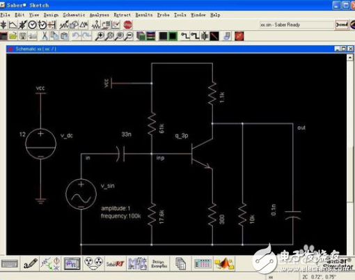
Before the saber simulation circuit, the circuit diagram should be drawn first. How to draw the circuit diagram is described below.
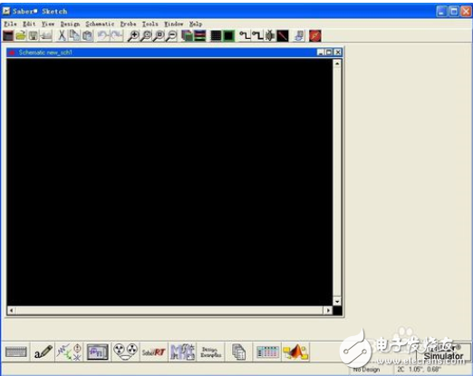
1. Open the saber software.
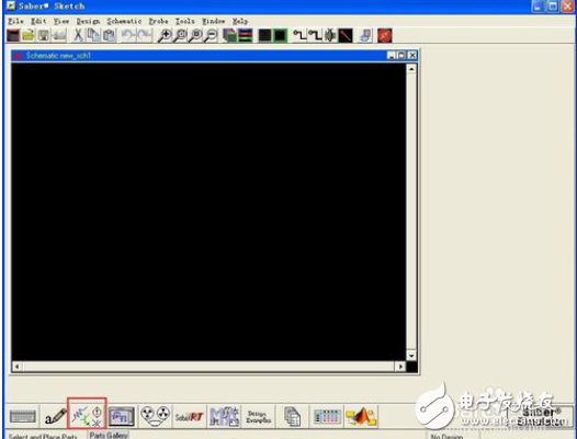
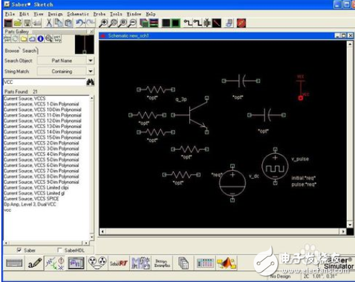
2. Click on the next line of tools, PartsGallery, or select the menu SchemaTIc-Getpart-PartsGallery.
3. Enter the meta symbol, double click on the component, or drag the component to place it on the right interface.
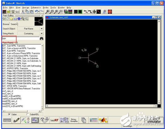
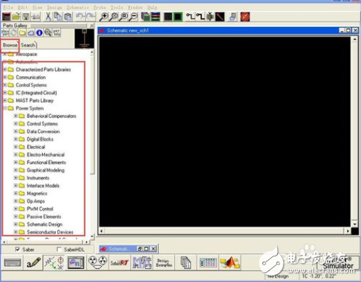
4. If you want a certain type of component, you can choose it in the big category below Browse.
5. Place all required components in accordance with the above method.
6. Position the components and press the W key to connect. During the pendulum component, press Ctrl+r to toggle the component.
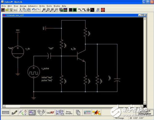
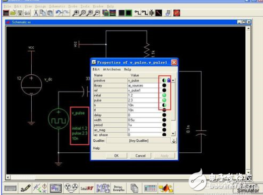
7. After the component is connected, click on the component opt ​​to modify the component parameters.
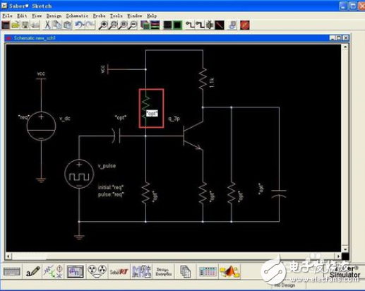
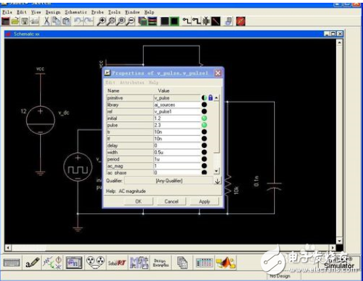
8. If there are more power parameters, you can double-click the component and modify the corresponding parameters in the dialog box that comes out.
9. If the component parameters are to be displayed, click the black dot on the right side of the right dialog box. All black is not displayed, half black and half green, showing value value, all green is displayed with Name and Value.
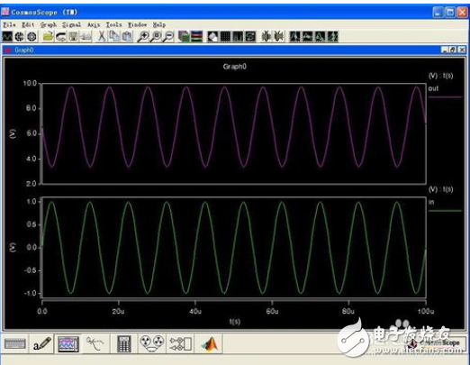
The main thing of the saber simulation circuit is to look at the voltage and current waveforms at certain points of the circuit. When the simulation is done, the waveform is obtained. How to deal with the waveform is better to analyze the circuit? The following is introduced.
Method / step1. Open the saber software and analyze the circuit with some analysis method to get the waveform.
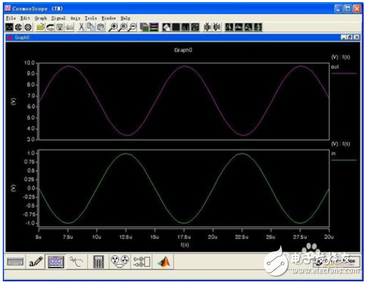
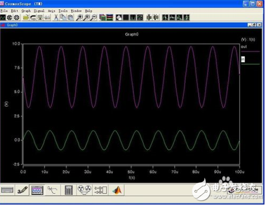
2. Pull out the computer waveform you want to watch in the running CosmosScope software. The following figure shows the input and output waveforms.
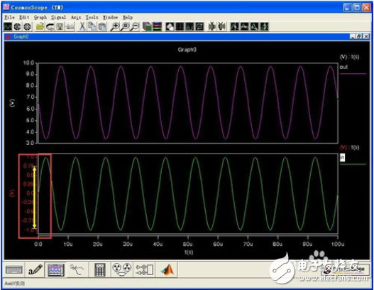
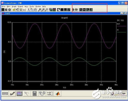
3. Press the mouse on the X axis and drag it. You can also drag the mouse within the waveform, but this method is difficult to control.
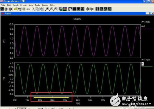
4. This will change the X-axis time. The length of time is related to the length of the drag.
5, change the voltage scale on the Y axis is the same method
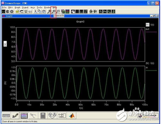
6. Waveform restore Press the Zoomtofit icon.
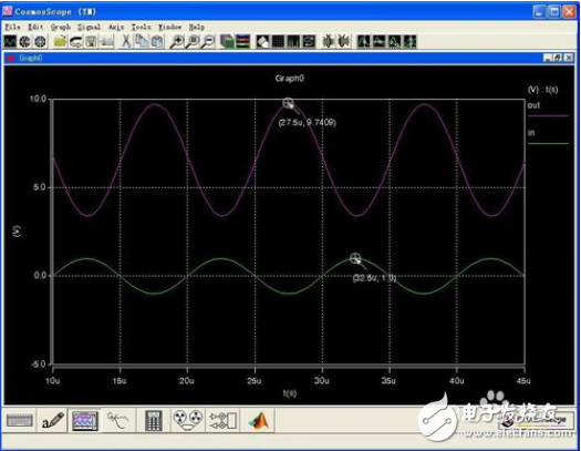
7. The two waveforms can move and move the same coordinate for comparison. Just move according to the marker line.
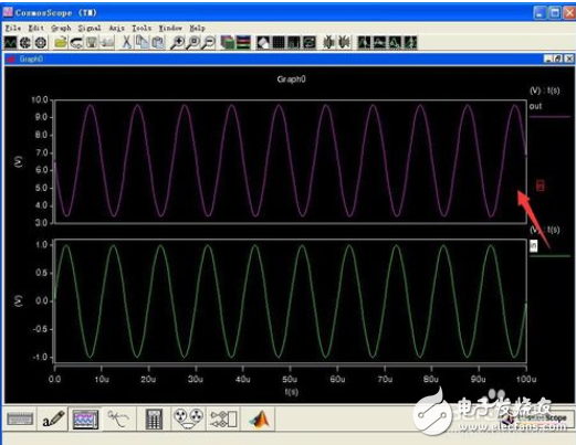
8. Release it to another waveform coordinate.
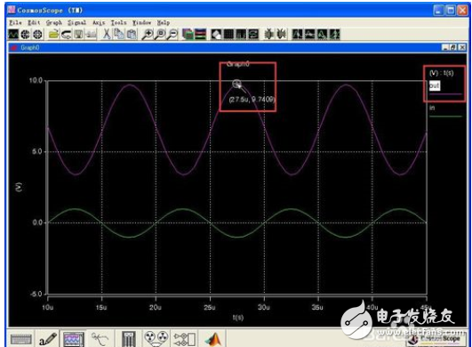
9, the last few icons on the menu bar are test waveform related data, such as the maximum point and the like.
10. Select the waveform to be marked first, then click the icon.
11. We see from the waveform that the output is 10 times larger than the input and is in the opposite direction to the input, which is the characteristic of this circuit.
Zinc rod high purity of over 99.995% was widely used in vacuum coating and other purposes.
Zinc Rod,Pure Zinc Rod,Zinc Anode Rod,Zinc Welding Rod
Shaoxing Tianlong Tin Materials Co.,Ltd. , https://www.tianlongspray.com