The 74LS138 is a 3-wire-8-line decoder with pinouts as follows.
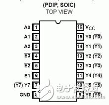
A0~A2: address input
STA (E1): strobe
/STB(/E2), /STC(/E3): strobe (active low)
/Y0~/Y7: Output (active low)
VCC: Power supply is positive
GND: ground
A0~A2 corresponds to Y0——Y7;
A0, A1, A2 are input in binary form, and then converted into decimal, corresponding to the corresponding Y number output low level, the others are high level;
Based on two 74LS138 microcontroller I / O port expansion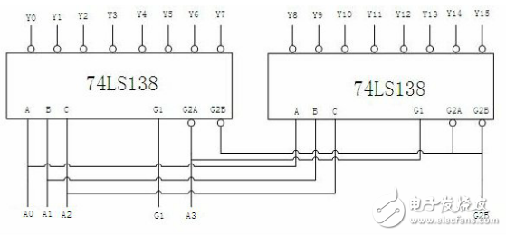
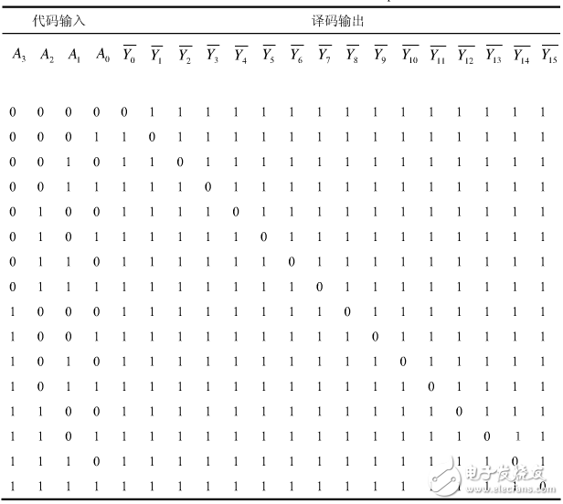
The two 74LS138 chips are connected as shown in the above figure to realize the expansion of the I/O port of the AT89C51 chip. Among them, the enable terminal G1 selects a high level, and G2b selects a low level. The four input ports A0~A3 are respectively connected with P1.0~P1.3 of the AT89C51 of the single-chip microcomputer to realize the chip select function of the AD9835 chip; the Y0~Y15 end is used for output. According to the above figure, you can get the corresponding truth table, as shown in the following table.
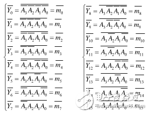
According to the truth table composed of the above two 74LS138 chips, the corresponding logical expression can be obtained:
The corresponding Protel circuit connection diagram is as shown. Among them, the enable input terminals G1 and G2b of the first 74LS138 chip are loaded with high level and low level respectively, and the enable input terminal G2a is provided by the P1.3 end of the AT89C51 single chip microcomputer. When the P1.3 terminal provides a low level, the 74LS138 chip is in the working state; when the P1.3 terminal provides a high level, the 74LS138 chip is in an inoperative state. The output station Y0~Y7 is used to provide the chip select signal (FSYNC) of the chip AD9835.
Similarly, for the second 74LS138 chip, the enable inputs G2a and G2b are loaded with a low level, and the enable input G1 is provided by the P1.3 terminal of the AT89C51 microcontroller. When the P1.3 terminal provides a high level, the 74LS138 chip is in the working state; when the P1.3 terminal provides a low level, the 74LS138 chip is in an inoperative state. Therefore, through the connection of the above two 74LS138 chips, the expansion function of "4-terminal input-16-terminal output" can be realized. The output terminals Y8~Y11 are used to provide the chip select signal (FSYNC) of the chip AD9835.
Alarm Accessories,Alarm Products,Alarm Equipment
Chinasky Electronics Co., Ltd. , https://www.chinacctvproducts.com