Field-programmable gate array FPGAs often process large amounts of data, and data storage becomes a problem. With SPI Flash's large capacity, fast read/write speed, low cost, and no loss of data after power-off, configuration data can be configured. Stored in SPI Flash [1]. It saves a lot of I/O port resources compared to the traditional parallel bus interface Flash, which provides more possibilities for system function expansion. Therefore, a design method of FPGA-based SPI Flash controller is proposed, which is implemented by Verilog HDL. The simulation and verification results are obtained in Isim. The final application is successfully applied in the self-designed VGA display control circuit, and can be extended. To all similar systems [2].
1 system overall designThe Spartan-6 family of xc6slx9 chips in the FPGA package is packaged in tqg-144, which provides up to 400MHz operating clocks, up to 5 720 efficient dual-register 6-input look-up tables (LUTs) and a rich set of built-in System-level modules, built on proven 45 nm low-power copper process technology, provide the perfect balance of price/performance and power. The chip has 9152 logic elements, 32 18 kbyte block RAM blocks, 16 18-I 18-bit embedded multipliers, 2 phase-locked loops (PLLs) and 4 clock management blocks (DCM). In this 144-pin tqg package FPGA, users can use 102 I/Os [3] to meet the needs of this system.
The configuration chip used in the Flash chip is Winbond's W25Q80BV series 8 M bit capacity SPI Flash. The chip consists of 16 parts, each with 256 pages and 256 bytes per page. The chips feature advanced write protection and a maximum clock rate of 50 MHz for reading data. Operating from 2.7 V to 3.6 V, with overall erase and sector erase, flexible page programming instructions, and write protection, data is stored for at least 20 y (year), and each sector can withstand 100 000 wipes Write loop. SPI Flash has power-down save capability. When the system is powered on, the FPGA first reads the programming data from the configuration chip SPIFlash and loads the FPGA. The HOLD# and WP# pins of SPIFlash should be connected with pull-up resistors. Because the pins are high-impedance when the FPGA is powered up, if there is no such pull-up resistor, the HOLD# and WP# inputs of FLASH are floating, there is no certain The level, which in turn causes the data bus level to be undefined, is not allowed.
The system consists of serial port, FPGA and SPI Flash. The overall block diagram of the system is shown in Figure 1.
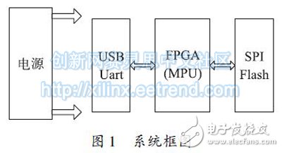
In Figure 1, the FPGA is the core of the circuit. On the one hand, it receives data from the serial port of the PC and writes the data into the Flash. On the one hand, it reads data from the Flash; on the other hand, it generates various control signals required by the system. As a field-programmable device, the FPGA can easily burn a program to change its function, so it can be used during design debugging. The bit file is burned into the FPGA for online debugging. The mc file program is directly downloaded into SPI Flash for functional verification.
2 FPGA internal module designThe top-level file of the FPGA consists of seven modules, as shown in Figure 2.
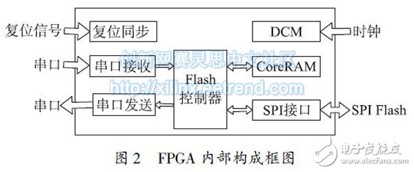
In Figure 2, the reset signal is mainly to synchronize the external reset signal; the DCM module is mainly to multiply and manage the clock; the serial port receiving module buffers the data obtained from the serial port to the FIFO; the flash control module mainly controls the reading and writing of the external SPI Flash. The data obtained from the serial port is stored in the SPI Flash, and the data in the SPI Flash is continuously sent to the serial port sending module; the CoreRAM is an IP core dedicated to Xilinx, and is used for buffering the internal data of the FPGA in this design; the SPI interface module Provides a serial clock for SPI Flash and enables serial-to-parallel conversion of data. When the upper layer user sends an instruction to store the configuration data of the FPGA into the SPI Flash, the configuration data is output from the serial port receiving module to the flash module, and the flash module continuously extracts the data into the CoreRAM, and the data in the CoreRAM is written into the SPI Flash through the flash module. in. When the system is re-powered to configure the FPGA, the data in the SPI Flash is read into the Flash module, the data in the Flash module is cached in the CoreRAM, and finally the data in the CoreRAM is extracted to the corresponding module in the upper layer. Configuration of the FPGA.
From the above analysis, we can know that the data flow inside the FPGA is very clear, and the relationship between the modules is also very clear, so the division of this block diagram is scientific. If the overall block diagram is not well defined, the possibility of successful debugging is very small. In addition, if you want to change the way the data is obtained during the upgrade, just replace the serial port receiving module with a new program; if you want to change the data display mode, just replace the serial port sending module with a new one. The implementation of each functional module is described below.
2. 1 serial port receiving and transmitting part
The serial port sending and receiving parts are similar. The serial port receiving part sends the serial port data from the PC to the flash controller, and the serial port sending part sends the data read from the flash to the PC, which is the reverse process of the serial port receiving. Take the serial port transmission part as an example for analysis. The block diagram of the serial port receiving module is shown in Figure 3.
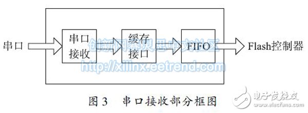
Figure 3 contains three sub-modules. The serial port receiving module receives data from the PC serial port. In order to make the speed as fast as possible, the designed baud rate is 115 200 bit / s; the cache interface is mainly to buffer the data received by the serial port. To FIFO; FIFO is a module that is instantiated and used as a data cache.
Nantong Boxin Electronic Technology Co., Ltd. , https://www.ntbosen.com