In practice, it is necessary to deal with increasing radio frequency interference (RFI), especially for long signal transmission lines and low signal strength, which is typical for instrumentation amplifiers because of their inherent common-mode rejection. Capability, which extracts weaker differential signals from stronger common mode noise and interference. However, there is a potential problem that is often overlooked, that is, the RF rectification problem existing in the instrumentation amplifier. When there is strong RF interference, the integrated circuit may rectify the interference and then exhibit the DC output offset error. The common-mode signal at the input of the instrumentation amplifier is typically attenuated by its common-mode rejection. RF rectification still occurs because even the best instrumentation amplifiers do not actually reject common mode noise at signal frequencies above 20 kHz. The input stage of the amplifier may rectify the strong RF signal and then exhibit the DC offset error. Once rectified, the low-pass filter at the output of the instrumentation amplifier will not eliminate this error. If the RF interference is intermittent, it can cause undetectable measurement errors.
The most practical solution for designing a practical RFI filter to solve this problem is to use a differential low-pass filter in front of the instrumentation amplifier to attenuate the RF signal. The filter has three functions: to eliminate as much of the RF energy as possible in the input line; to balance the AC signal between each line and ground (common); and to maintain a sufficiently high input impedance throughout the measurement bandwidth to Avoid increasing the load on the signal source.
Figure 1 is a basic block diagram of various differential RFI filters. The component values ​​shown in the figure are all selected for the AD8221. The typical bandwidth of the AD8221 is -3dB: 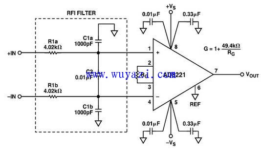
Figure 1 Low-pass filter circuit for preventing RF interference rectification error
1MHz, typical voltage noise level is 7 nVQQ screenshot 20141204111321.jpg. In addition to suppressing RF interference, the filter also has input overload protection. Because resistors R1a and R1b help isolate the instrumentation amplifier input circuitry from external sources.
2 is a simplified diagram of the anti-radio frequency interference circuit. As can be seen from the figure, the filter forms a bridge circuit whose output is connected across the input pins of the instrumentation amplifier. In view of this connection method, any mismatch between the two time constants of C1a/R1a and C1b /R1b will result in bridge imbalance, thereby reducing high frequency common mode rejection. Therefore, the resistors R1a and R1b and the capacitors C1a and C1b should always be equal. 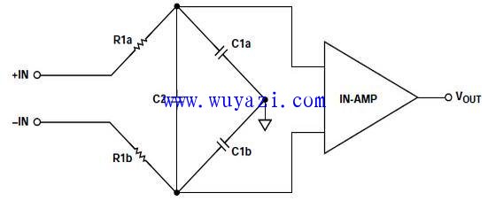
Figure 2 Capacitor C2 forms the bypass of C1a/C1b and can effectively reduce the AC common-mode rejection error caused by component mismatch. As shown in the figure, C2 is connected across the output of the bridge, so that C2 is actually associated with C1a. The series combination of C1b is in a parallel relationship. When connected in this way, C2 can effectively reduce any AC common mode rejection errors caused by mismatch. For example, if C2 is 10 times larger than C1, this connection will reduce the common-mode rejection error due to C1a/C1b mismatch to one-twentieth. It should be noted that this filter does not affect DC common mode rejection.
RFI Suppression Circuitry for AD620 Series Instrumentation Amplifiers Figure 3 shows the circuit for general purpose instrumentation amplifiers (such as the AD620 series). Compared to the AD8221 series, these instrumentation amplifiers have higher noise levels (12 nVHz) and lower bandwidth. . Accordingly, this type of instrumentation amplifier uses the same input resistance, but the value of capacitor C2 is increased approximately five times to 0.047 F to provide sufficient RF attenuation. Using the values ​​shown in the figure, the -3 dB bandwidth of the circuit is approximately 400 Hz; by reducing the resistance of R1 and R2 to 2.2 k, the bandwidth can be increased to 760 Hz. It is important to note that increasing bandwidth is a price The circuit driver in front of the instrumentation amplifier is required to have a lower impedance load, which will reduce the input overload protection performance to some extent. 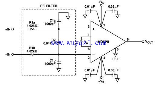
Figure 3. RFI Suppression Circuitry for AD620 Series Instrumentation Amplifiers RFI Suppression Circuitry for Micropower Instrumentation Amplifiers Some instrumentation amplifiers are more susceptible to RF rectification than other amplifiers, requiring a stronger filter. A good example is a micropower instrumentation amplifier (such as the AD627) with a lower input current. A simple method of increasing the value of two resistors R1a/R1b and/or the value of capacitor C2 can increase RF attenuation, but at the expense of reduced signal bandwidth. Since the AD627 instrumentation amplifier has higher noise (38nV Hz) than a general-purpose integrated circuit (such as the AD620 series device), an input resistor with a higher resistance value can be used without significantly reducing the noise performance of the circuit. Figure 4 shows the modification of the basic RC anti-radio interference circuit shown in Figure 1, using an input resistor with a higher resistance value. 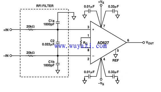
Figure 4 The RFI suppression circuit for the AD627 has a filter bandwidth of approximately 200 Hz. With a gain of 100 and an input of 1V pp, the maximum dc offset voltage is approximately 400 VRTI over the 1 Hz to 20 MHz frequency range. When the gain is constant, the RF signal rejection of the circuit (output RF level / input RF level) will be better than 61 dB.
RFI Filter for the AD623 Instrumentation Amplifier Figure 5 shows the RFI immunity circuit recommended for use with the AD623 instrumentation amplifier. Since this device is less susceptible to RF interference than the AD627, the input resistor can be reduced from 20 kΩ to 10 kΩ, which increases the signal bandwidth of the circuit and reduces the noise contribution of the resistor. In addition, 10k resistors provide extremely efficient input protection. When using the values ​​shown in the figure, the bandwidth of the filter is about 400 Hz. When the gain is 100 and the input is 1Vp-p, the maximum dc offset voltage is less than 1 V. When the gain is constant, the RF signal suppression of the circuit is better than 74. dB. 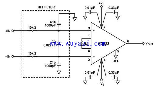
Figure 5 AD623 RFI Suppression Circuit
AD8225 RFI Filter Circuit Figure 6 shows the recommended RFI filter for this instrumentation amplifier. The AD8225 instrumentation amplifier has a fixed gain of 5 and is more susceptible to RF interference than the AD8221. If an RFI filter is not used, the dc offset voltage measured by this instrumentation amplifier is approximately 16 mV RTI when inputting a 2 Vp-p, 10 Hz to 19 MHz sine wave. By using a resistor with a higher resistance value, the filter can achieve higher RF attenuation than the AD8221 circuit: 10 k instead of 4 k. This is acceptable due to the high noise level of the AD8225. If a filter is used, the dc offset voltage error is negligible. 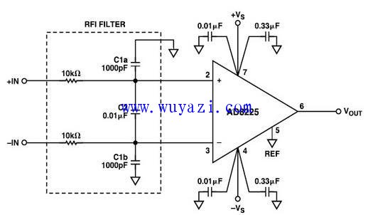
Figure 6 AD8225 RFI filter circuit uses a common-mode RF choke as an instrumentation RF interference filter as an alternative to the RC input filter. A commercial common-mode RF choke can be connected in front of the instrumentation amplifier, as shown in Figure 7. Shown. The common mode choke is a two-way winding RF choke using a shared core. Any common mode input RF signal at both inputs is attenuated by the choke. The common mode choke provides a simple RF interference suppression method with a small number of components, while obtaining a wider signal passband, but the effectiveness of this method depends on the quality of the common mode choke used. A well-matched choke inside. Another potential problem with using chokes is that they do not improve input protection like RC RFI filters. With an RF choke and an AD620 instrumentation amplifier with a nominal gain of 1000, the circuit shown in Figure 7 reduces the dc offset voltage to less than 4.5 V RTI when a 1 Vp-p common mode sine wave is input. The high frequency common mode rejection ratio is also greatly reduced, as shown in Table I.
Ceramic Housing
Ceramic Housing
YANGZHOU POSITIONING TECH CO., LTD. , https://www.cnpositioning.com